
Diamond Electron Emission Cathode, Electron Emission Source, Electron Microscope, and Electron Beam Exposure Device

a technology of electron beam and emission cathode, which is applied in the manufacture of discharge tube main electrodes, electrode systems, electric discharge tubes/lamps, etc., can solve the problems of frequent operation, short service life of discharge tubes, and frequent replacement operations, etc., and achieves low cost, high throughput, and small energy width

Inactive Publication Date: 2008-02-28
SUMITOMO ELECTRIC IND LTD
View PDF11 Cites 3 Cited by
  • Summary
  • Abstract
  • Description
  • Claims
  • Application Information

AI Technical Summary

Benefits of technology

[0037] With the present invention, it is possible to realize a high-efficiency electron emission cathode and electron emission source that is suitable for devices of all types using electron beams, such as vacuum tubes, electron beam analyzers, accelerators, electron beam irradiation devices for sterilization, X-ray generators, irradiation devices for resins, and electron beam heating devices. In particular, it is possible to realize an electron emission cathode and electron emission source that use diamond, have a high brightness and a small energy width and are suitable for electron microscopes and electron beam exposure devices. Furthermore, by using the electron emission cathode and electron emission source, it is possible to realize an electron microscope enabling high-magnification observations and an electron beam exposure device in which fine patterns can be drawn at a high throughput.

Problems solved by technology

However, although W filaments are inexpensive, a problem associated therewith is that the service life thereof is extremely short (about 100 hours).
The resultant problem is that a replacement operation such as opening a vacuum container to the atmosphere or adjusting the optical axis of electron beam when the filament is broken has to be frequently performed.
The service life of LaB6 is about 1000 hours and longer than that of W filaments, but because it is used in devices in which beams with a comparatively high brightness are obtained, the replacement operation is most often performed by the device manufacturers and the cost thereof is high.
A problem associated with ZrO / W that has a comparatively long service life (about one year) and W with a sharpened tip that allows a higher brightness to be obtained is that the replacement cost is high.
Further, because the operation temperature is low, a long service life can be expected.

Method used


Image

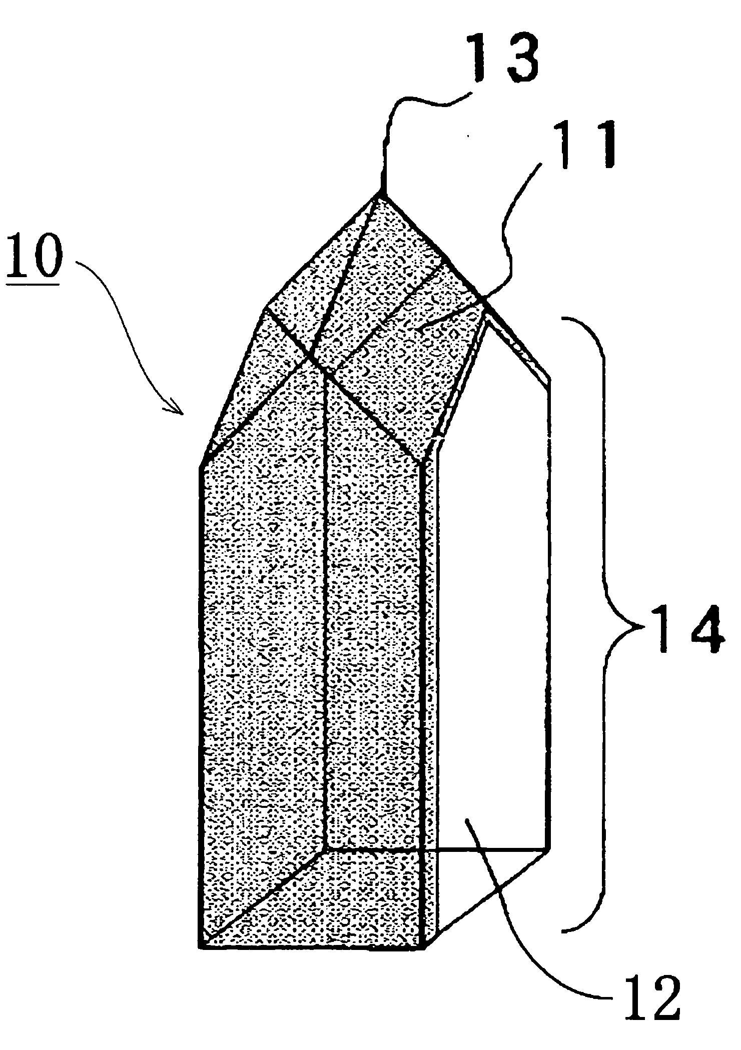
  • Diamond Electron Emission Cathode, Electron Emission Source, Electron Microscope, and Electron Beam Exposure Device
  • Diamond Electron Emission Cathode, Electron Emission Source, Electron Microscope, and Electron Beam Exposure Device
  • Diamond Electron Emission Cathode, Electron Emission Source, Electron Microscope, and Electron Beam Exposure Device

Examples


example 1

[0076] The diamond electron emission cathode, electron emission source, electron microscope, and electron beam exposure device in accordance with the present invention will be described below in greater detail based on Examples thereof.

[0077] The samples with numbers (1) to (23) were fabricated as diamond electron emission cathodes. All the samples had a size of 0.6 mm×0.6 mm×2.5 mmt and an aspect ratio of about 4.2. A single crystal p-type semiconductor diamond synthesized by vapor phase growth was prepared as the second semiconductor and shaped by laser machining and polishing. Then, the second semiconductor was used as a substrate and an n-type semiconductor diamond that is the first semiconductor, or an intrinsic semiconductor diamond that is the third semiconductor was epitaxially grown thereupon by vapor phase growth. The p-type impurity of the p-type semiconductor diamond was boron. Single crystals with a B concentration of 4×1019 cm−3 were used for all the samples. The samp...

example 2

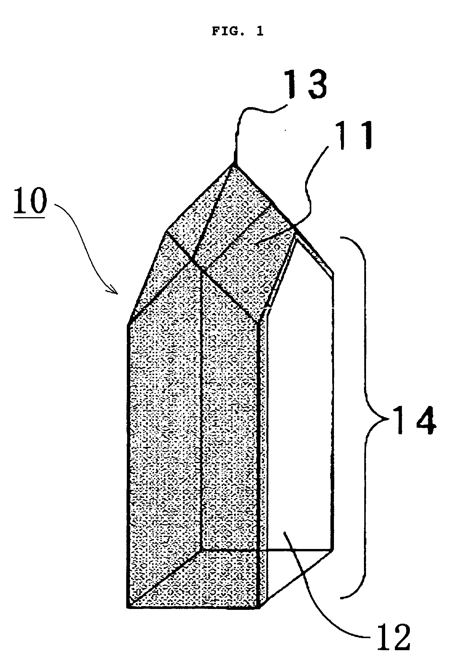
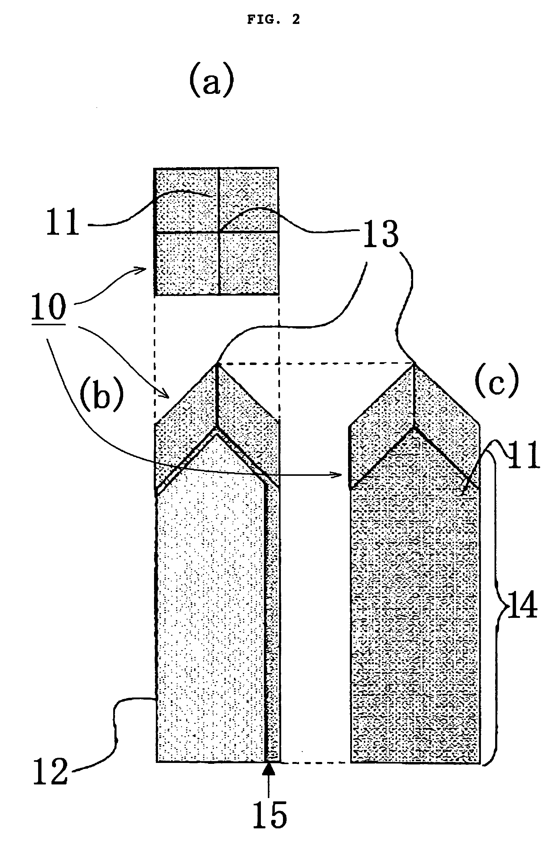
[0082] The samples with numbers (24) to (46) were fabricated as diamond electron emission cathodes. All the samples had a size of 0.6 mm×0.6 mm×2.5 mmt and an aspect ratio of about 4.2. A single crystal p-type semiconductor diamond synthesized by vapor phase growth was prepared as the second semiconductor and shaped by laser machining and polishing. Then, the second semiconductor was used as a substrate and an n-type semiconductor diamond that is the first semiconductor, or an intrinsic semiconductor diamond that is the third semiconductor was epitaxially grown thereupon by vapor phase growth. The p-type impurity of the p-type semiconductor diamond was B. Single crystals with a B concentration of 4×1019 cm−3 were used for all the samples. The samples with numbers (24), (27), (28), (31), (32), (35), (36), (39), (40) to (46) were used to fabricate diamond electron emission cathodes such as the cathode shown in FIG. 1, the samples with numbers (25), (29), (33), (37) were used to fabric...


PUM


Abstract

An object is to provide an electron emission cathode and an electron emission source using diamond and having a high brightness and a small energy width that are suitable for electron ray and electron beam devices and vacuum tubes, in particular, electron microscopes and electron beam exposure devices, and also electronic devices using such cathode and source. A diamond electron emission cathode according to the present invention has single crystal diamond in at least part thereof, the diamond electron emission cathode having a columnar shape formed by a sharpened acute section and a heating section, being provided with one electron emitting portion in the sharpened acute section, and being constituted of at least two types of semiconductors that differ in electric properties. One of the types constituting the semiconductors is an n-type semiconductor containing n-type impurities at 2×1015 cm3 or higher, the other one is a p-type semiconductor containing p-type impurities at 2×1015 cm-3 or higher, the p-type semiconductor and the n-type semiconductor are joined together, the heating section is energized parallel to the junction surface and directly heated by a pair of current introducing terminals, and some of the introduced electrons are emitted from the electron emitting portion.

Description

RELATED APPLICATIONS [0001] This application is the U.S. National Phase under 35 U.S.C. §371 of International Application No. PCT / JP2006 / 31262 filed Jun. 19, 2006, which claims the benefit of Japanese Application Nos. 2005-178163 filed Jun. 17, 2005, 2005-257452 filed Sep. 6, 2005, and 2005-257791 filed Sep. 6, 2005, the disclosures of which Applications are incorporated by reference herein.TECHNICAL FIELD [0002] The present invention relates to a diamond electron emission cathode and an electron emission source for use in electron ray and electron beam devices such as electron microscopes and electron beam exposure devices and also in vacuum tubes such as traveling wave tubes and microwave tubes and also to electronic devices using such cathode and source. BACKGROUND ART [0003] Because an electron bears a negative charge and has a very small mass, electron beams in which electrons are arranged to travel in one direction have the following special features. (1) The direction and the...

Claims


Application Information

Patent Timeline
Patent Type & Authority Applications(United States)
IPC IPC(8): H01J1/15
CPCH01J1/14H01J1/15H01J2237/06316H01J2237/06308H01J37/06
Inventor UEDA, AKIHIKOYAMAMOTO, YOSHIYUKINISHIBAYASHI, YOSHIKIIMAI, TAKAHIRO
Owner SUMITOMO ELECTRIC IND LTD
Learn More