
Diamond Electron Emission Cathode, Electron Emission Source, Electron Microscope, And Electron Beam Exposure Device

a technology of electron beam and emission cathode, which is applied in the manufacture of discharge tube main electrodes, electrode systems, electric discharge tubes/lamps, etc., can solve the problems of high replacement cost, high service life of discharge tubes, and high cost of discharge tubes, and achieves high throughput, small energy width, and high brightness

Inactive Publication Date: 2008-07-10
SUMITOMO ELECTRIC IND LTD
View PDF13 Cites 2 Cited by
  • Summary
  • Abstract
  • Description
  • Claims
  • Application Information

AI Technical Summary

Benefits of technology

[0045]With the present invention, it is possible to realize an electron emission cathode and electron emission source that use diamond and have a high brightness and a small energy width and suitable for electron beam and electron beam devices and vacuum tubes, in particular electron microscopes and electron beam exposure devices. Furthermore, by using the electron emission cathode and electron emission source, it is possible to realize an electron microscope enabling high-magnification observations and an electron beam exposure device in which fine patterns can be drawn at a high throughput.

Problems solved by technology

However, although W filaments are inexpensive, a problem associated therewith is that the service life thereof is extremely short (about 100 h).
The service life of LaB6 is about 1000 h and longer than that of W filaments, but because it is used in devices in which beams with a comparatively high brightness are obtained, the replacement operation is most often performed by the device manufacturers and the cost thereof is high.
A problem associated with ZrO / W that has a comparatively long service life of about one year and W with a sharpened tip that allows a higher brightness to be obtained is that the replacement cost is high.
Further, because the operation temperature is low, a long service life can be expected.

Method used


Image

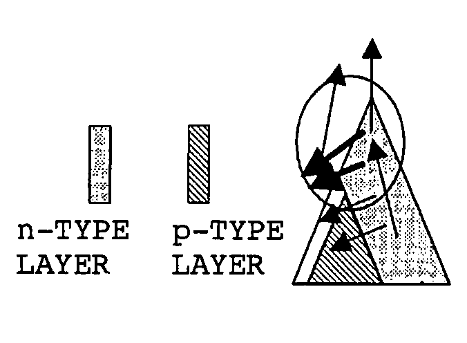
  • Diamond Electron Emission Cathode, Electron Emission Source, Electron Microscope, And Electron Beam Exposure Device
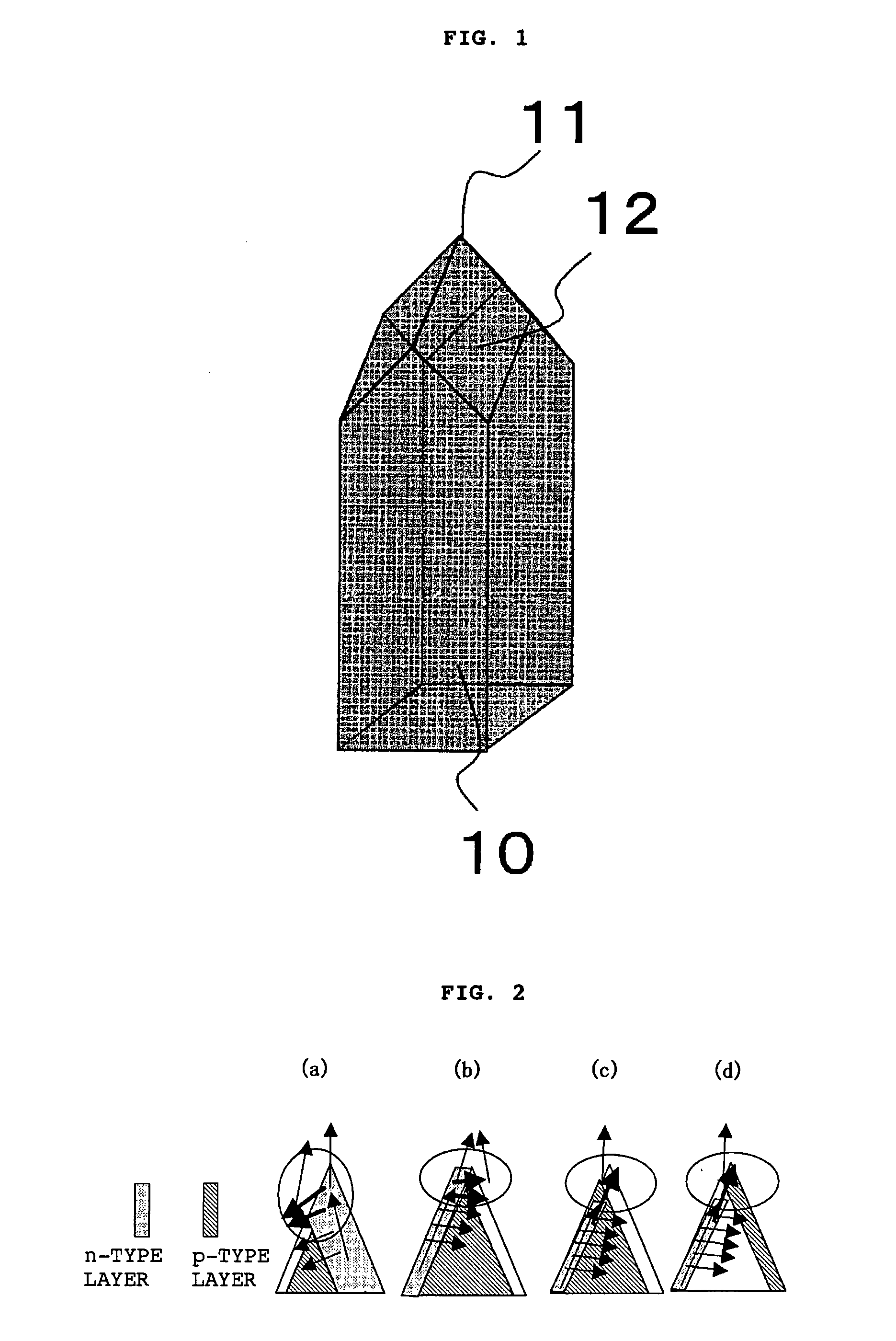
  • Diamond Electron Emission Cathode, Electron Emission Source, Electron Microscope, And Electron Beam Exposure Device
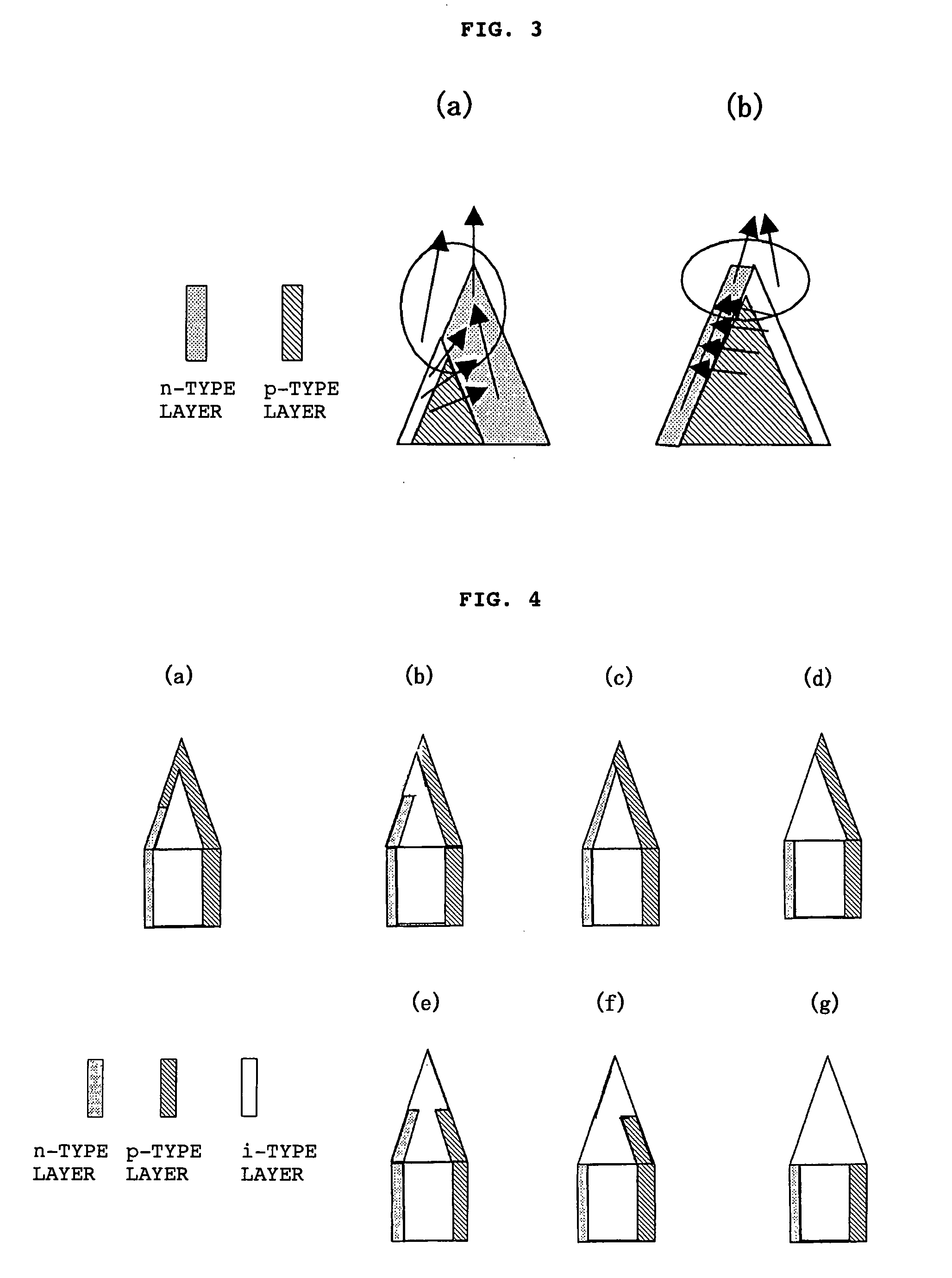
  • Diamond Electron Emission Cathode, Electron Emission Source, Electron Microscope, And Electron Beam Exposure Device

Examples


example 1

[0077]Single crystal diamond substrates obtained by high-pressure synthesis and single crystal substrates obtained by vapor phase synthesis, all having the shape of an elongated rectangular parallelepiped, were subjected to sharpening in order to prepare samples having a sharp tip end, as shown in FIG. 10(a). Diamonds subjected to doping of various types were synthesized on those substrates. The synthesis of diamonds was conducted by a microwave CVD method by using hydrogen gas and methane gas.

[0078]The tip end diameter could be roughly adjusted during polishing, and representative samples with a tip end diameter of about 1 μm and about 10 μm were prepared. The tip end can be also sharpened to a submicron level by diamond re-growth or vertical etching using plasma or ions.

[0079]When an n-type layer was formed on the (111) plane, the methane concentration (CH4 / H2), phosphorus concentration (PH3 / CH4), pressure and substrate temperature were set to 0.03-0.05%, 0.002-20%, 100 Torr and 8...

example 2

[0089]Single crystal diamond substrates obtained by high-pressure synthesis and single crystal substrate obtained by vapor phase synthesis, all having the shape of an elongated rectangular parallelepiped, were subjected to sharpening in order to prepare samples having a sharp tip end, as shown in FIG. 12(a)-(d). Diamonds subjected to doping of various types were synthesized on those substrates. The synthesis of diamonds was conducted by a microwave CVD method by using hydrogen gas and methane gas.

[0090]The tip end diameter could be roughly adjusted during polishing, and representative samples with a tip end diameter of about 1 μm and about 10 μm were prepared. The tip end can be also sharpened to a submicron level by diamond re-growth or vertical etching using plasma or ions.

[0091]The conditions of forming a n-type layer on the (111) plane, forming a n-type layer on the (100) surface, and forming a p-type film were identical to those of Example 1.

[0092]All the substrates were boron-...

example 3

[0101]As shown in FIG. 14(a), (b), samples were prepared in which the tip end of the samples had been sharpened in the same manner as in Example 1. The difference between this example and Example 1 was that an i-type layer that was not doped with impurities was formed prior to the formation of the n-type layer. In all other aspects, the structures were identical, and the tests were carried out under the same doping conditions.

[0102]With this method chips having with a tip end in the form of an n-type layer and a pin stack were fabricated.

[0103]Similarly to Example 1, a sample in which a boron-doped p-type layer was formed prior to the formation of the i-type layer was also prepared. Although similar structures of a pin-stack type were obtained, the advantage of the latter structure was that the junction surface could use a CVD film in which the impurities of the p-type layer were accurately controlled. Another feature identical to that of Example 1 was that the produced samples in w...


PUM


Abstract

An object of the present invention is to provide an electron emission cathode and an electron emission source using diamond and having a high brightness and a small energy width that are used in electron beam and electron beam devices and vacuum tubes, in particular, electron microscopes and electron beam exposure devices, and electronic devices that uses such electron emission cathode and electron emission source. A diamond electron emission cathode according to the present invention has single crystal diamond in at least part thereof, the diamond electron emission cathode being in a columnar form having a sharpened acute section in one place of an electron emitting portion and being constituted by at least two types of semiconductors that differ in electric properties. One of the types constituting the semiconductors is a n-type semiconductor comprising n-type impurities at 2×1015 cm−3 or higher, the other type is a p-type semiconductor comprising p-type impurities at 2×1015 cm−3 or higher, the p-type semiconductor and the n-type semiconductor are joined, an electric potential that is negative with respect to the p-type semiconductor is applied with a pair of current introducing terminals to the n-type semiconductor so that electrons flow from the n-type semiconductor to the p-type semiconductor, and the n-type semiconductor has a component in which electrons flow to the electron emitting portion.

Description

TECHNICAL FIELD[0001]The present invention relates to a diamond electron emission cathode and an electron emission source for use in electron beams and electron beam devices such as electron microscopes and electron beam exposure devices and in vacuum tubes such as traveling wave tubes and microwave tubes, and also relates to an electronic device using such cathode and source.BACKGROUND ART[0002]Because an electron bears a negative charge and has a very small mass, electron beams in which electrons are arranged to travel in one direction have the following special features. (1) The direction and the degree of convergence can be controlled by an electric or magnetic field. (2) Energy in a wide range can be obtained by acceleration and deceleration with an electric field. (3) Because the wavelength is short, the beam can be converged to a small diameter. Electron microscopes and electron beam exposure devices employing such special features have been widely used. As cathode materials ...

Claims


Application Information

Patent Timeline
Patent Type & Authority Applications(United States)
IPC IPC(8): H01J1/14H01L29/16
CPCH01J1/14H01J1/15H01J2237/06316H01J2237/06308H01J37/06
Inventor NISHIBAYASHI, YOSHIKIUEDO, AKIHIKOYAMAMOTO, YOSHIYUKIIMAI, TAKAHIRO
Owner SUMITOMO ELECTRIC IND LTD
Learn More