Fabricating method for printed circuit board

a printed circuit board and fabrication method technology, applied in the direction of resist details, conductive pattern formation, electric connection formation of printed elements, etc., can solve the problems of defective entire board, general cost of molds, and only the bottom surface of the insulation layer of the circui

Inactive Publication Date: 2008-03-06
SAMSUNG ELECTRO MECHANICS CO LTD
View PDF25 Cites 28 Cited by
  • Summary
  • Abstract
  • Description
  • Claims
  • Application Information

AI Technical Summary

Benefits of technology

[0013]An aspect of the invention is to provide a method of fabricating a printed circuit board, in which the circuit is buried, so that there is no peeling of the circuit, and in which fine-line circuits can be formed.
[0015]Still another aspect of the invention is to provide a method of fabricating a printed circuit board, in which the efficiency of reducing fabrication costs can be increased by utilizing equipment used in existing printed circuit board fabrication processes.
[0016]Yet aspect of the invention is to provide a method of fabricating a printed circuit board, which provides a superb level of evenness and which allows easy heat release.
[0017]Another aspect of the invention is to provide a method of fabricating a printed circuit board, with which interlayer connections can readily be implemented with low costs.

Problems solved by technology

One possible drawback of conventional circuit forming methods may be that, since a circuit made from copper is formed on the insulation layer, the portion attached to the insulation layer is only the bottom surface of the circuit.
Thus, when forming a fine-line circuit, undercuts may occur at the attachment portions between the circuit and the resin, whereby the fine-line circuit may be peeled off.
Such peeling off would cause the entire board to be defective.
However, in the imprinting method, the mold is generally expensive, and there is much difficulty in separating the mold from the insulation layer after transcribing the patterns on the mold.
Also, curing the resin while the mold is being pressed may cause the pressing to be very time-consuming, and may cause lowered productivity.
With the laser processing, not only is the equipment itself highly expensive, but also the method may require expensive aluminum masks or dielectric masks for forming the circuit.
However, with mechanical hole processing, the abrasion of the bit may cause increased costs, and with B2it, the use of paste for interlayer connection renders B2it as yet unreliable for use in semiconductor substrates, and there is a limit to how minute the holes can be made.
Also, since NMBI physically connects copper with copper, there may be problems in contact reliability.

Method used


Image

  • Fabricating method for printed circuit board
  • Fabricating method for printed circuit board
  • Fabricating method for printed circuit board

Examples


Embodiment Construction

[0053]The method of fabricating a printed circuit board according to certain embodiments of the invention will be described below in more detail with reference to the accompanying drawings, in which those components are rendered the same reference numeral that are the same or are in correspondence, regardless of the figure number, and redundant explanations are omitted.

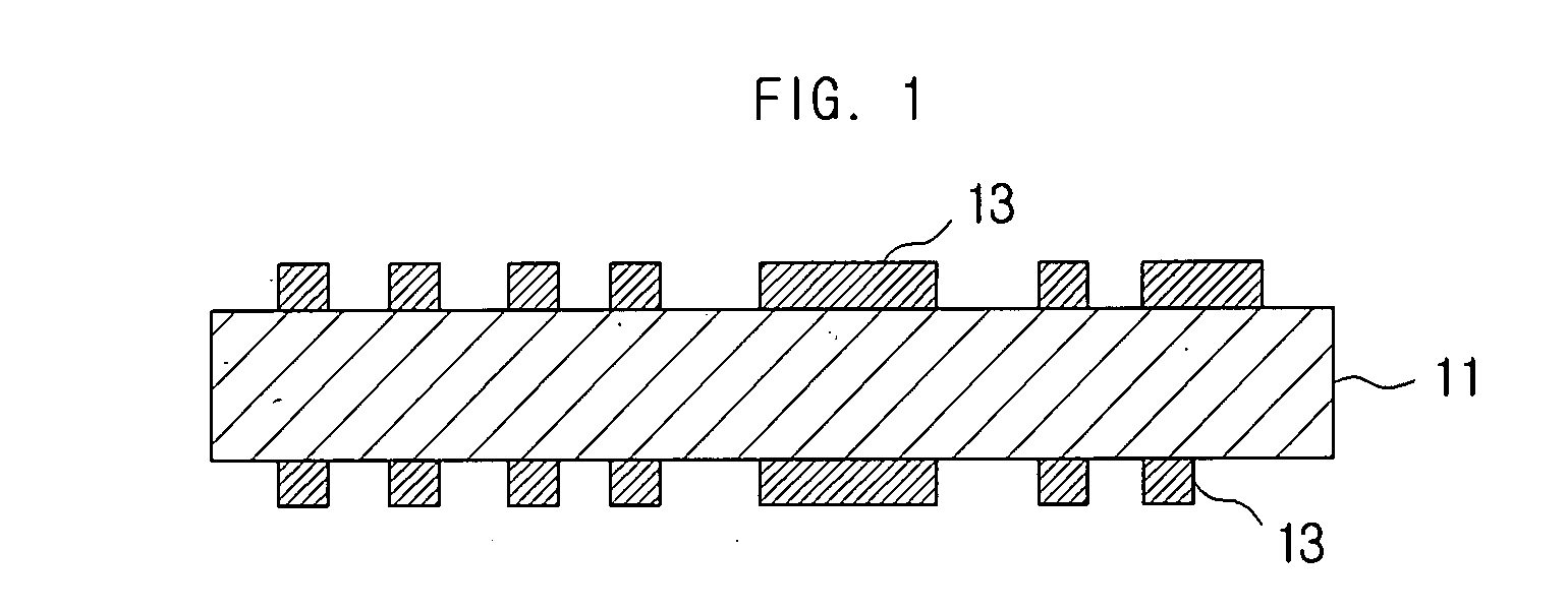
[0054]FIG. 1 is a cross-sectional view illustrating a core layer used in a method of fabricating a printed circuit board according to an embodiment of the invention.

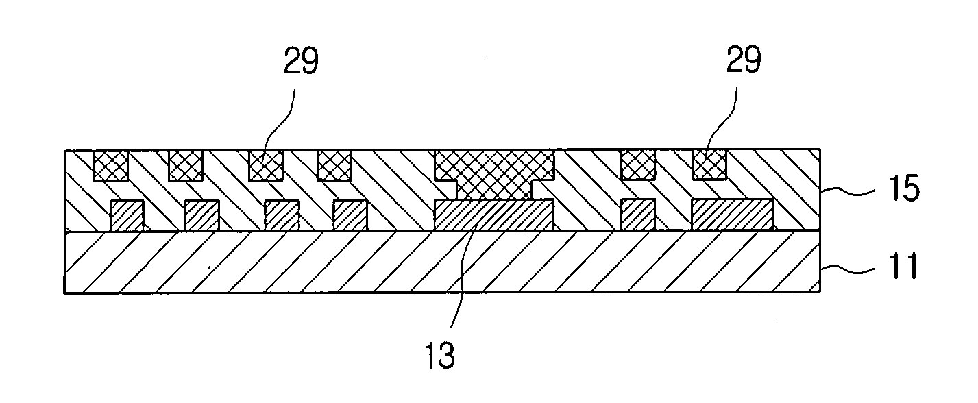
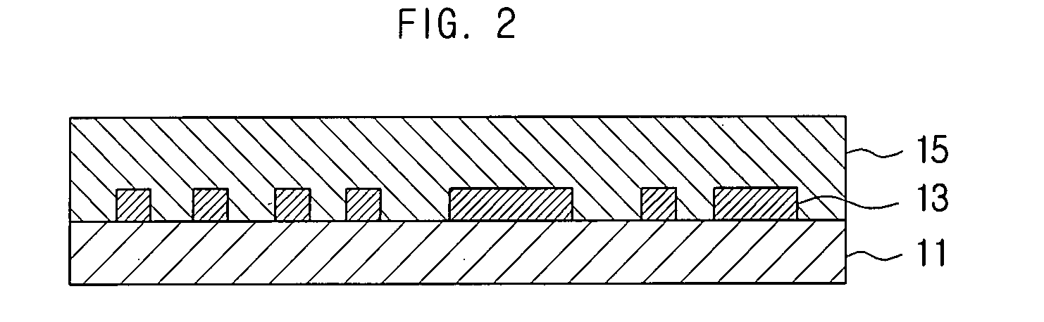
[0055]Referring to FIG. 1, an inner circuit 13 may be formed on either side of a core layer 11. While there are inner circuits 13 formed on both sides of the core layer 11 in FIG. 1, in some cases there may be just one inner circuit formed only on one side. Because the inner circuit 13 may be embedded between insulation layers in a subsequent process, there may be no undercuts as occurring in conventional fine-line circuits. The inner circuit 13 may be ele...


PUM

PropertyMeasurementUnit
temperatureaaaaaaaaaa
electricallyaaaaaaaaaa

Abstract

A method of fabricating a printed circuit board is disclosed. A method of fabricating a printed circuit board that includes: stacking an insulation layer on at least one surface of a core layer, on which an inner circuit is formed, and forming an outer circuit pattern; burying the outer circuit pattern in the insulation layer; removing the outer circuit pattern to form minute grooves and curing the insulation layer; and forming an outer circuit by filling metal in the minute grooves, makes it possible to readily form high-resolution fine-line circuits, as well as to reduce fabrication costs and increase productivity.

Description

CROSS-REFERENCE TO RELATED APPLICATIONS[0001]This application claims the benefit of Korean Patent Application No. 10-2006-0085789 filed with the Korean Intellectual Property Office on Sep. 6, 2006, the disclosure of which is incorporated herein by reference in its entirety.BACKGROUND[0002]1. Technical Field[0003]The present invention relates to a method of fabricating a printed circuit board.[0004]2. Description of the Related Art[0005]With mobile electronic equipment rapidly trending towards lighter, smaller, and thinner products that provide higher performance, and with the demands for LSI packages having higher speeds and higher densities, there is currently a demand also for higher-density build-up boards. Currently, in a flip chip board, the mainstream is to use a SAP (semi-additive process) in forming the circuits, in order to increase the wiring density of the board. However, there is ongoing research on methods other than SAP methods, for conveniently forming fine-line circu...

Claims


Application Information

Patent Timeline
Patent Type & Authority Applications(United States)
IPC IPC(8): H05K3/02
CPCH05K3/0014Y10T29/49165H05K3/045H05K3/06H05K3/107H05K3/20H05K3/205H05K3/426H05K3/4614H05K3/465H05K3/4658H05K2201/0361H05K2201/0376H05K2201/09036H05K2201/09563H05K2203/0278H05K2203/0384H05K2203/0582H05K2203/1152H05K2203/1189H05K2203/308Y10T29/49126Y10T29/49155Y10T29/49156H05K3/0017H05K3/42
Inventor WATANABE, RYOICHIMIN, BYOUNG-YOULYOO, JE-GWANGKIM, JOON-SUNGKIM, SEUNG-CHULKANG, MYUNG-SAN
Owner SAMSUNG ELECTRO MECHANICS CO LTD
Why Eureka
Try Eureka