Method for driving light-emitting diode, light-emitting diode, method for driving display, display, method for driving electronic device, electronic device, method for driving optical communication apparatus, and optical communication apparatus

a technology of light-emitting diodes and diodes, which is applied in the direction of electric variable regulation, process and machine control, instruments, etc., to achieve the effects of stable emission wavelength, stable color reproduction, and wide dynamic rang

Active Publication Date: 2008-03-06
SONY CORP
View PDF3 Cites 7 Cited by
  • Summary
  • Abstract
  • Description
  • Claims
  • Application Information

AI Technical Summary

Benefits of technology

[0041] According to the above embodiments of the present invention, a light-emitting diode can be driven with stable emission wavelength irrespective of drive current density. A display including the light-emitting diode can therefore achieve a wide dynamic range, stable color reproduction, and a wide color reproduction range. In particular, a method for driving the light-emitting diode can be used in combination with PWM to achieve a wider dynamic range than achieved only by PWM, a reduction in PWM frequency, and simplified signal processing in, for example, luminance correction. This allows for a reduction in the load on a signal-processing circuit and a drive circuit. Thus, the embodiments of the present invention can provide advantages from many viewpoints, including gradation, color reproduction range, cost, and signal processing. In addition, an optical communication apparatus including the light-emitting diode can achieve stable emission wavelength to enable highly reliable optical communication or transmission.

Problems solved by technology

This phenomenon results from localized carriers of indium atoms and a piezoelectric field due to lattice mismatch in a wurtzite crystal structure.

Method used


Image

  • Method for driving light-emitting diode, light-emitting diode, method for driving display, display, method for driving electronic device, electronic device, method for driving optical communication apparatus, and optical communication apparatus
  • Method for driving light-emitting diode, light-emitting diode, method for driving display, display, method for driving electronic device, electronic device, method for driving optical communication apparatus, and optical communication apparatus
  • Method for driving light-emitting diode, light-emitting diode, method for driving display, display, method for driving electronic device, electronic device, method for driving optical communication apparatus, and optical communication apparatus

Examples


example

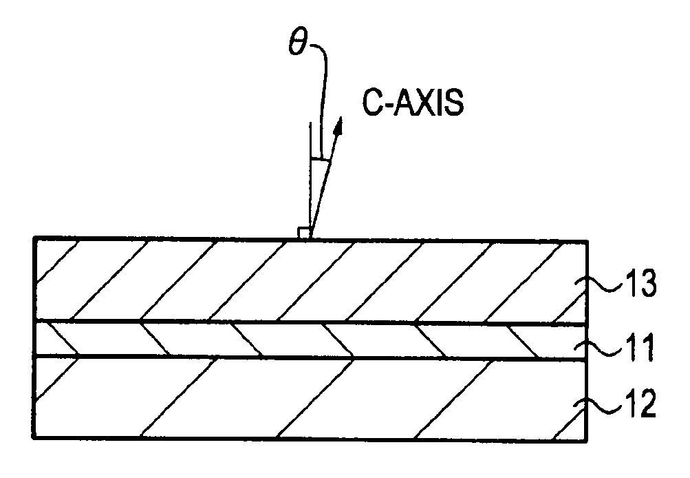
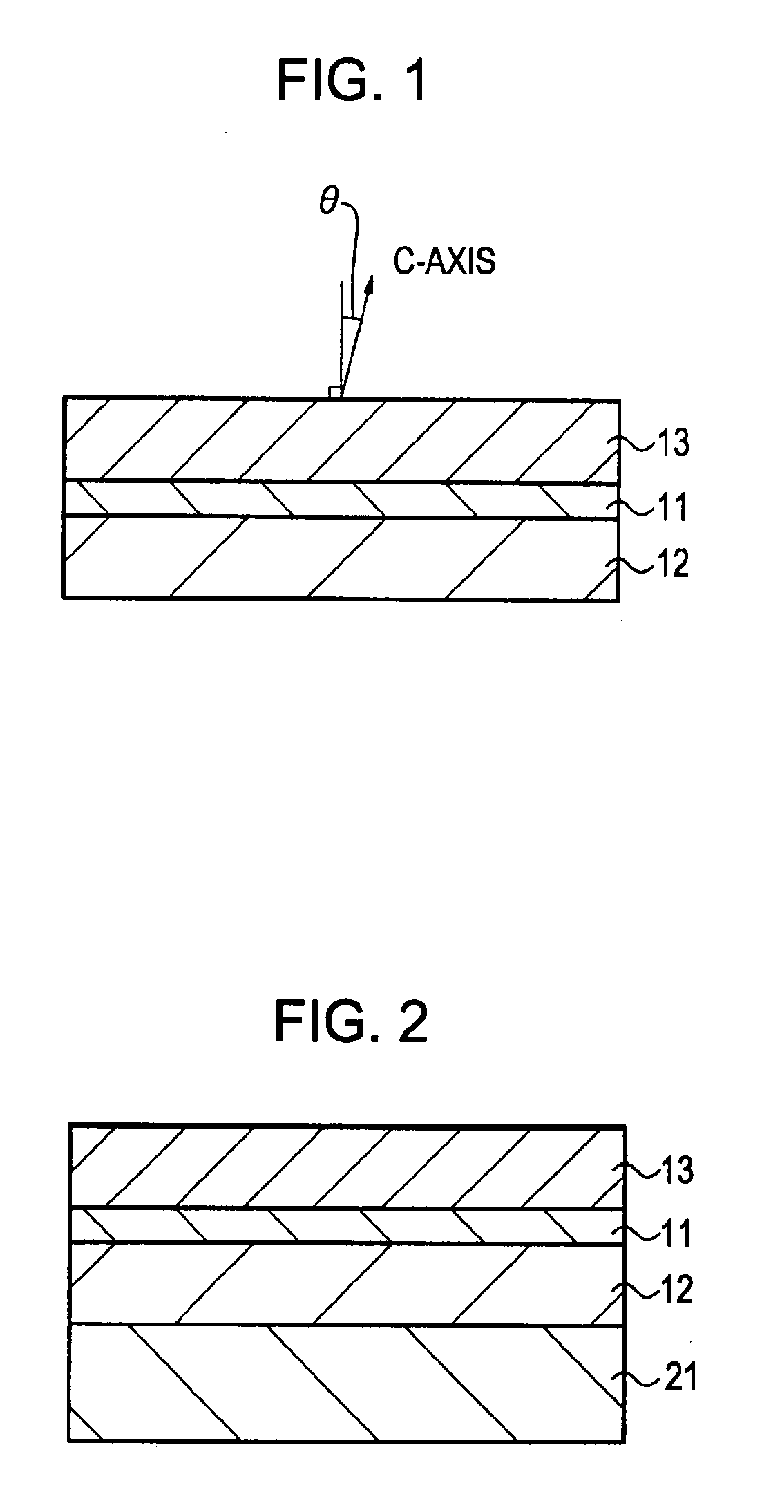
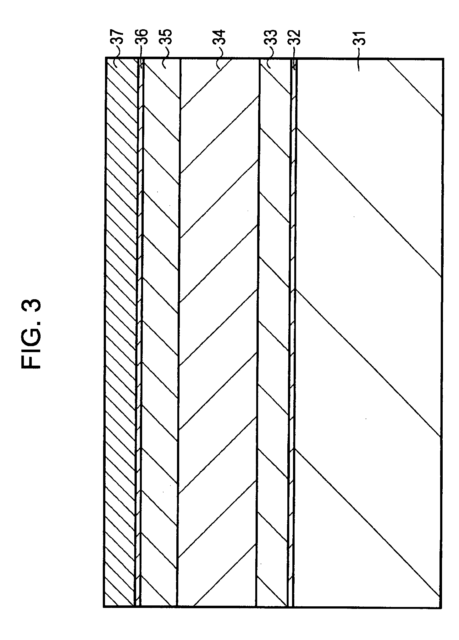
[0065] Referring to FIG. 3, vicinal sapphire substrates 31 having main surfaces inclined at angles θ of 0.2°, 0.3°, 0.4°, and 0.6° with respect to the c-plane were used as the vicinal substrate 21, and GaN-based semiconductor layers were grown thereon to form light-emitting diode structures.

[0066] In FIG. 3, each vicinal sapphire substrate 31 was introduced into a reactor of an MOCVD apparatus. A surface of the vicinal sapphire substrate 31 was cleaned in a hydrogen atmosphere at a substrate temperature of 1,050° C. for ten minutes. The substrate temperature was then lowered to 500° C. Supply of ammonia (NH3) into the reactor as a nitrogen (N) source was started, and trimethylgallium (TMG) was supplied as a gallium (Ga) source to deposit a low-temperature-grown GaN buffer layer 32 to a thickness of 20 nm. After the supply of TMG was stopped, the substrate temperature was raised to 1,020° C. with ammonia being supplied. The supply of TMG was then restarted, so that a GaN layer 33 st...


PUM


Abstract

A method for driving a light-emitting diode includes the step of modulating the luminance of the light-emitting diode with current density within the range of 20 A/cm2 or less. The light-emitting diode includes a p-type layer, an n-type layer, and a light-emitting layer disposed therebetween and having an indium-containing quantum well structure. Each of the p-type layer, the n-type layer, and the light-emitting layer includes a nitride-based group III-V compound semiconductor crystal having a wurtzite structure. The light-emitting layer has a main surface inclined at an angle of 0.25° to 2° with respect to a c-plane.

Description

CROSS REFERENCES TO RELATED APPLICATIONS [0001] The present invention contains subject matter related to Japanese Patent Application JP 2006-219583 filed in the Japanese Patent Office on Aug. 11, 2006, the entire contents of which are incorporated herein by reference. BACKGROUND OF THE INVENTION [0002] 1. Field of the Invention [0003] The present invention relates to methods for driving light-emitting diodes, light-emitting diodes, methods for driving displays, displays, methods for driving electronic devices, electronic devices, methods for driving optical communication apparatuses, and optical communication apparatuses. In particular, the present invention relates to methods for driving light-emitting diodes suitable for applications such as a variety of displays including InGaN / GaN-based light-emitting diodes. [0004] 2. Description of the Related Art [0005] InGaN / GaN-based light-emitting diodes, particularly ones with emission wavelengths in the visible region, can vary in emissi...

Claims


Application Information

Patent Timeline
Patent Type & Authority Applications(United States)
IPC IPC(8): H01L33/00H05B37/02H01L33/06H01L33/24H01L33/32H05B44/00
CPCG09G3/3216G09G3/3225G09G2320/0233H05B33/0857H01L33/16H01L33/32H04N9/3155G09G2320/0626H05B45/20
Inventor BIWA, GOSHI
Owner SONY CORP
Why Eureka
Try Eureka