Light emitting diode with adjustable light colors and preparation method therefor

A light-emitting diode and light color technology, which is applied in the direction of electrical components, circuits, semiconductor devices, etc., can solve the problem of low radiation recombination efficiency of LEDs, and achieve the effect of improving radiation recombination efficiency

Inactive Publication Date: 2016-06-29
INST OF SEMICONDUCTORS - CHINESE ACAD OF SCI
View PDF11 Cites 11 Cited by
  • Summary
  • Abstract
  • Description
  • Claims
  • Application Information

AI Technical Summary

Problems solved by technology

[0005] In view of this, the purpose of the present invention is to disclose a light-color adjustable light-emitting diode and its preparation method to overcome the problems of low LED radiation recombination efficiency

Method used


Image

  • Light emitting diode with adjustable light colors and preparation method therefor
  • Light emitting diode with adjustable light colors and preparation method therefor
  • Light emitting diode with adjustable light colors and preparation method therefor

Examples


preparation example Construction

[0034] The present invention also provides a method for preparing light-color-tunable light-emitting diodes, comprising the following steps:

[0035] (1) Prepare the substrate;

[0036] (2) growing an epitaxial layer on the substrate, the epitaxial layer comprising a first multiple quantum well layer;

[0037] (3) Etching a number of micro-nano holes on the first multi-quantum well layer, the micro-nano holes running through the first multi-quantum well layer;

[0038] (4) epitaxially growing a second multi-quantum well structure in the micro-nano hole until it is flush with the upper surface of the first quantum well layer.

[0039] For the selection of the substrate, it may be a substrate commonly used in the preparation of LED technology, preferably a sapphire substrate, a silicon substrate, a gallium nitride substrate or a gallium oxide substrate.

[0040] For the specific process of step (3) photolithographic etching, it can be: on the first multi-quantum well layer, ep...

Embodiment 1

[0055] Embodiment 1 of the present invention will be described in detail below with reference to the accompanying drawings. This embodiment provides a method for manufacturing a single-chip white light-emitting diode with tunable light color and no phosphor powder. Include the following steps:

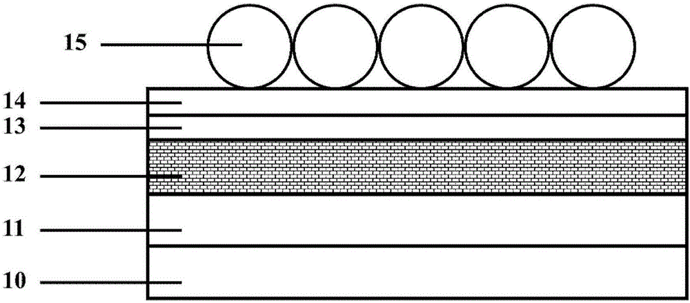
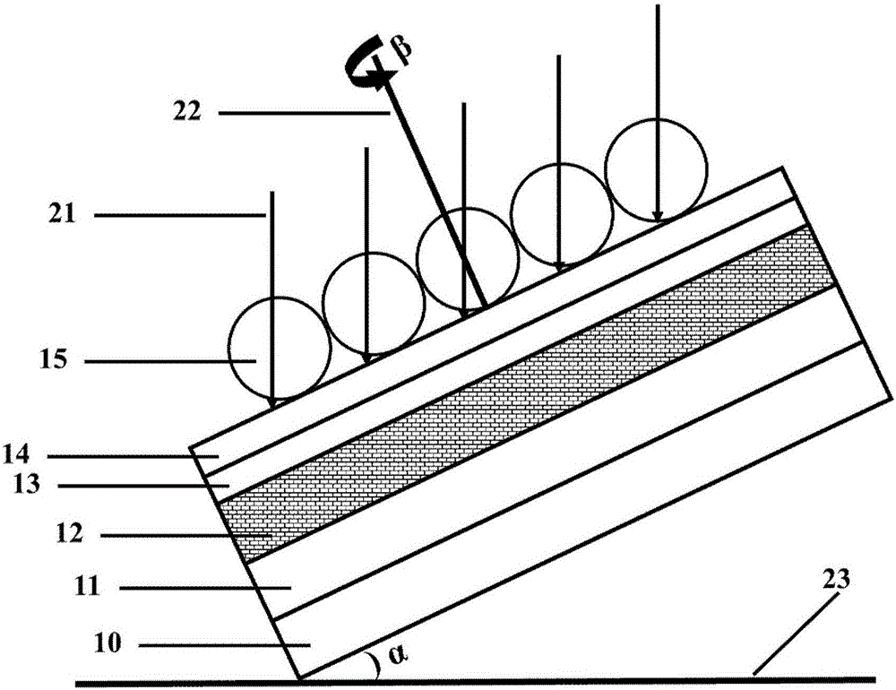
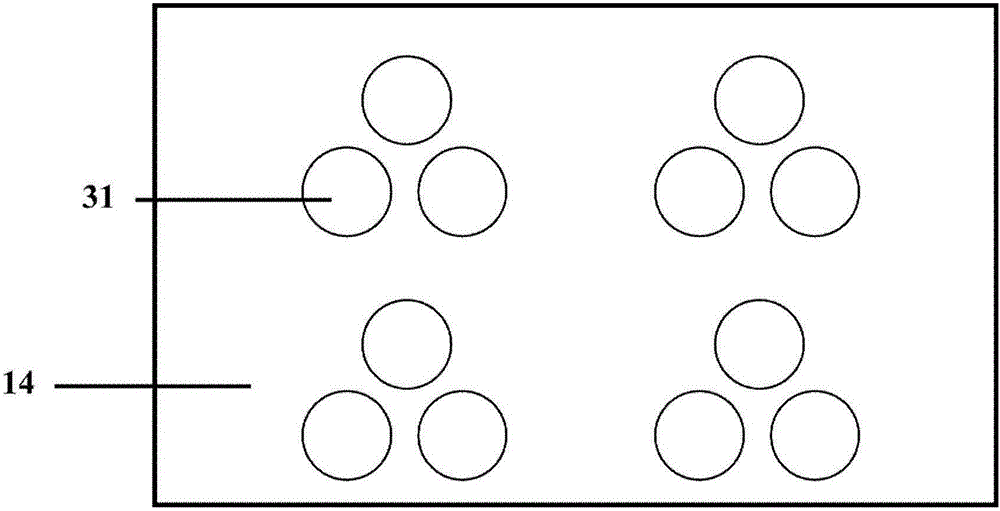
[0056] Step 1: On the sapphire substrate 10, epitaxially grow a buffer layer, an unintentionally doped gallium nitride layer, an n-type gallium nitride layer 11, and a blue multi-quantum well layer 12 sequentially by metal-organic chemical vapor deposition, and then use plasma A layer of 100-1000nm silicon dioxide insulating dielectric thin film passivation layer 13 is grown by volume-enhanced chemical vapor deposition (PECVD), and then a positive photoresist 14 is spin-coated on the 13, and the positive photoresist is formed by spin-coating or pulling method. Self-assembled single-layer polystyrene microspheres 15 on the resist 14, with a diameter of 100-10000 nm, such as figure 1 s...


PUM


Abstract

Disclosed is a light emitting diode with adjustable light colors. The light emitting diode comprises a substrate and an epitaxial layer, wherein the layer comprises a first multi-quantum-well layer; a micro-nano hole penetrating through the first multi-quantum-well layer is formed in the first multi-quantum-well layer; and a second multi-quantum-well layer flush with the lower surface of the first multi-quantum-well layer is deposited in the hole. The invention also provides a preparation method for the light emitting diode with the adjustable light colors. Different quantum wells are distributed in a transverse direction parallel to the substrate; the growth mode of the conventional longitudinally-stacked multi-quantum-well structure is changed, so that the problem of uneven distribution of electrons and holes in an active region of a longitudinally-stacked multi-quantum-well structured phosphor-powder-free single-chip white light emitting diode under a certain injection current is solved; and the light emitting diode with the adjustable light colors can be realized by different multi-quantum-well combinations.

Description

technical field [0001] The invention belongs to the technical field of semiconductors, and further relates to a light-color adjustable light-emitting diode and a preparation method thereof. Background technique [0002] Gallium nitride-based light-emitting diodes have the advantages of small size, high efficiency, long life, energy saving and environmental protection, and are expected to replace traditional light sources in the future and be used in general lighting and other fields. [0003] From the perspective of packaging, at present, there are two main methods to realize white LEDs: one is to combine multiple single-color LEDs to produce white light. However, due to the material system, driving voltage, and There are differences in temperature and light attenuation rate, and multiple sets of circuit designs are required to control the current separately, so this method is likely to cause design difficulties and increase costs; the other is to use blue LEDs to excite yel...

Claims


Application Information

Patent Timeline
Patent Type & Authority Applications(China)
IPC IPC(8): H01L33/06H01L33/32H01L33/00
CPCH01L33/06H01L33/0075H01L33/325
Inventor 熊卓魏同波王军喜李晋闽
Owner INST OF SEMICONDUCTORS - CHINESE ACAD OF SCI
Why Eureka
Try Eureka