Wiring pattern, electronic device, organic semiconductor device, layered wiring pattern, and layered wiring substrate using the wiring pattern

a technology of organic semiconductors and wiring patterns, applied in the direction of printed circuit manufacturing, printed circuit aspects, thermoelectric devices, etc., can solve the problems of increasing manufacturing costs, requiring expensive facilities, and affecting the effect of photolithography results

Inactive Publication Date: 2008-03-13
RICOH KK
View PDF15 Cites 16 Cited by
  • Summary
  • Abstract
  • Description
  • Claims
  • Application Information

AI Technical Summary

Benefits of technology

[0017]The present invention may provide a wiring pattern, an electronic device, an organic semiconductor device, a layered wiring pattern, and a layered wiri

Problems solved by technology

Conventionally, although photolithography methods are used for forming wirings of semiconductor devices and electronic circuits, the use of such photolithography methods requires expensive facilities.
Furthermore, the long and complicated procedures of the photolithography methods lead to an increase of manufacturing cost.
That is, in a case where wiring is formed by coating ink onto a water-repellent substrate, problems such as disconnection may occur due to a large portion of the ink concentrating at a bent corner part of the wiring while only a small portion of the ink is provided at areas other than the corner part.
Although the methods disclosed in Patent Documents 1 and 2 can prevent a concentration of liquid droplets from causing short-circuiting and disconnection in an in-plane direction (between linear patterns, between film patterns) of a substrate, the methods cannot prevent bulging of liquid droplets at an end part (corner part) of wiring with respect to a cross-sectional direction of the substrate (film thickness direction).
Therefore, in a case where an electrode pattern is provided on the above-described linear pattern or film pattern via an insulating layer, insulation failure may occur and result in short-circuiting of wires between the layers of a substrate.
Although the method disclosed

Method used


Image

  • Wiring pattern, electronic device, organic semiconductor device, layered wiring pattern, and layered wiring substrate using the wiring pattern
  • Wiring pattern, electronic device, organic semiconductor device, layered wiring pattern, and layered wiring substrate using the wiring pattern
  • Wiring pattern, electronic device, organic semiconductor device, layered wiring pattern, and layered wiring substrate using the wiring pattern

Examples


example 1

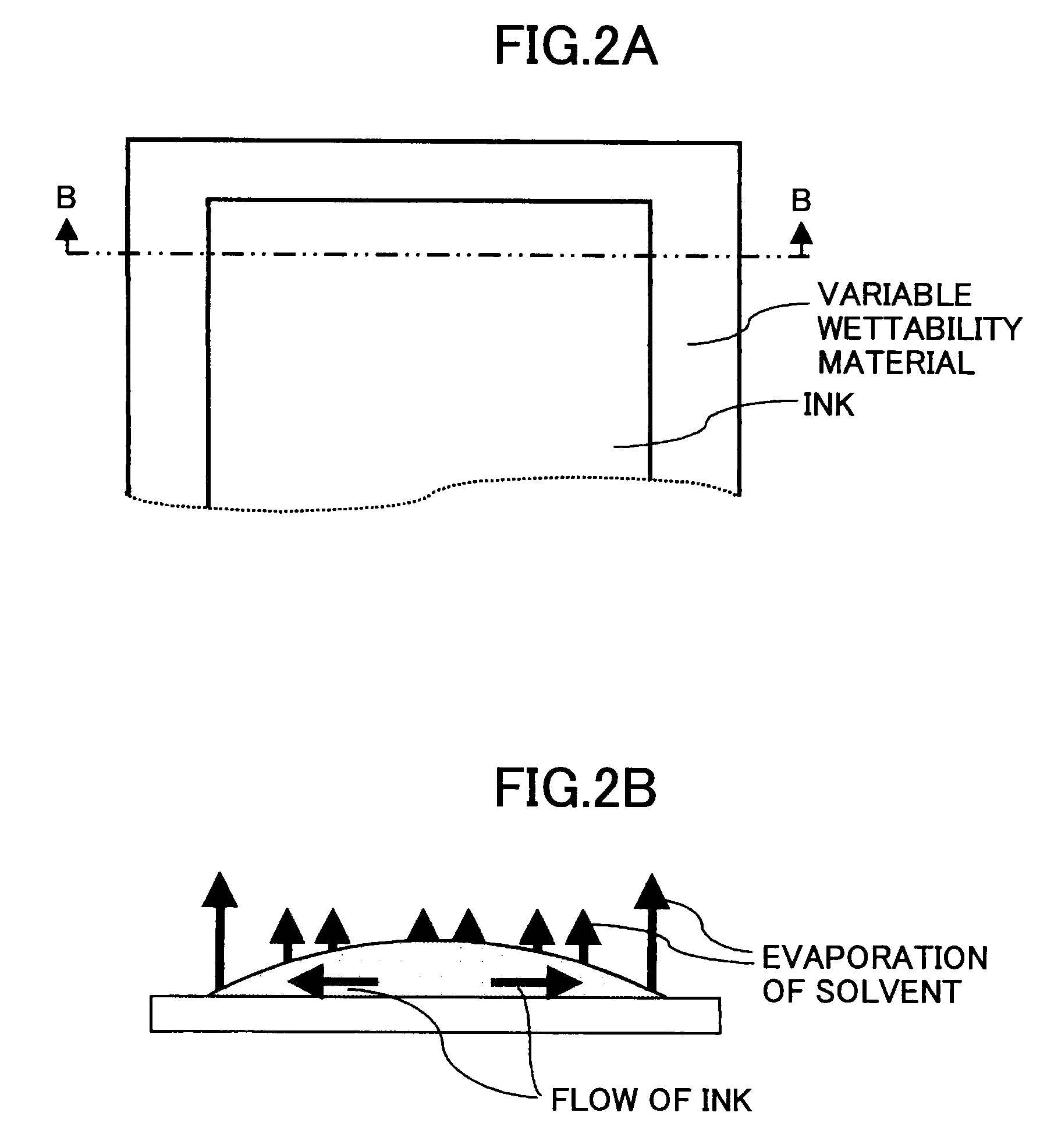
[0144]A variable wettability layer (hereinafter also referred to as “wettability control film”) is formed by applying a mixed solution having dissolved therein a precursor of the materials having a structure expressed with the below Formulas 6 and 7 onto a glass substrate by using a spin-coating method and baking the mixed solution in an environment of 280° C.

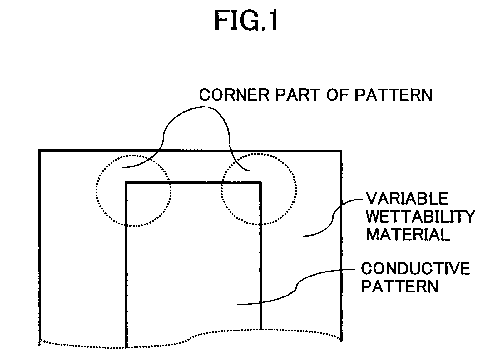
[0145]Then, a wettability area (high surface energy part) is formed on the variable wettability layer by using a mask having a pattern (opening(s)). The pattern of the mask is chamfered in a manner shown in FIG. 7A and has a line width of 80 μm and a chamfer length of 20 μm. In measuring the contact angle of the wettability area by using a silver nanoparticle ink, the wettability area exhibited a contact angle that is no greater than 5°.

[0146]Then, a conductive liquid (in this example, silver nanoparticle ink) is applied to the wettability area by using an inkjet method. Then, the variable wettability layer on which the silver ...

example 2

[0150]In Example 2, an insulating film is formed on the conductive pattern described in Example 1 (hereinafter referred to as “first conductive pattern layer”) by spin-coating polyimide onto the first conductive pattern layer and baking the coated configuration. Then, a second wettability control film formed of the same material as the Example 1 is formed on the insulating film. The combined thickness of the polyimide insulating film and the second wettability control film is 500 nm. Then, a wettability pattern (second wettability area) is formed on the second wettability control film by arranging a mask at a predetermined position on the second wettability control film and irradiating UV rays thereto. The mask is positioned so that the pattern of the second wettability control film intersects (overlaps) with the first pattern layer. Then, a silver nanoparticle ink is applied to the second wettability area by using an inkjet method. Then, the wettability control film on which the si...

example 3

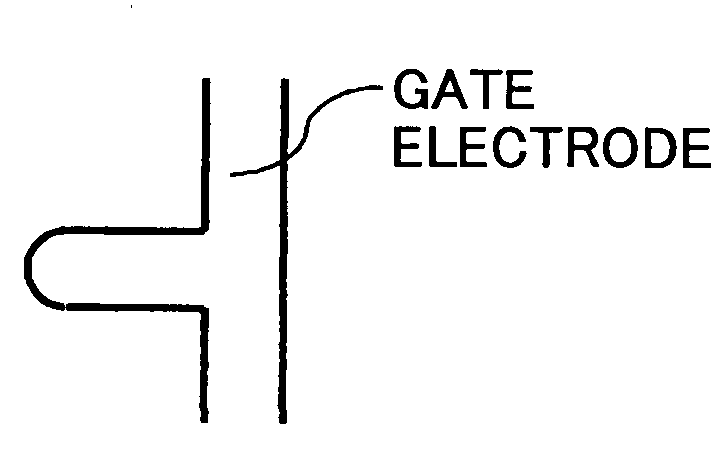
[0154]In Example 3, ten devices (in this example, thin film transistors (TFT)) having an electrode configuration shown in a plan view of FIG. 25B were fabricated under the below-described conditions.

[0155]First, as shown in FIG. 25A, a conductive pattern (gate electrode pattern) is formed by using the same material and method as those described in Example 1. The gate electrode pattern has a line width of 80 μm and a rounded chamfered part with a radius (R) of 40 μm. Then, a variable wettability layer (wettability control layer) is formed on the gate electrode pattern by spin-coating polyimide onto the gate electrode pattern and baking the coated configuration. Then, as shown in FIG. 25B, a source electrode pattern and a drain electrode pattern are formed on the variable wettability layer by arranging a mask at a predetermined position on the variable wettability layer and irradiating UV rays thereto.

[0156]Finally, a semiconductor layer is formed on the variable wettability layer by ...


PUM


Abstract

A wiring pattern is disclosed including: a variable wettability layer including a material whose critical surface tension changes in response to energy provided thereto, the wettability changing layer including a high surface energy part exhibiting a high critical surface tension and a low surface energy part exhibiting low critical surface tension; and a conductive pattern layer formed on the variable wettability layer at the high surface energy part. The conductive pattern layer has an elongated shape with a chamfered corner part in a plan view.

Description

BACKGROUND OF THE INVENTION[0001]1. Field of the Invention[0002]The present invention relates to a wiring pattern, an electronic device, an organic semiconductor device, a layered wiring pattern, and a layered wiring substrate using the wiring pattern, and more particularly to a shape of a conductive pattern of a wiring pattern and a configuration including the wiring pattern such as an electronic device, an organic semiconductor element, a layered wiring pattern, and a layered wiring substrate.[0003]2. Description of the Related Art[0004]Conventionally, although photolithography methods are used for forming wirings of semiconductor devices and electronic circuits, the use of such photolithography methods requires expensive facilities. Furthermore, the long and complicated procedures of the photolithography methods lead to an increase of manufacturing cost. Recently, a method of forming a wiring pattern by coating liquid containing conductive fine particles directly onto a substrate...

Claims


Application Information

Patent Timeline
IPC IPC(8): H01L51/00
CPCH01L51/0004H01L51/0018H01L51/0022H01L51/0541H05K2203/1173H05K3/1208H05K3/1241H05K2201/09272H01L51/0545H10K71/13H10K71/233H10K71/611H10K10/466H10K10/464
Inventor TOMONO, HIDENORIKAWASHIMA, IKUESUZUKI, KOEIAKIYAMA, YOSHIKAZU
Owner RICOH KK
Why Eureka
Try Eureka