

Semiconductor device and method of manufacturing the same
a technology of semiconductors and semiconductors, applied in the direction of semiconductor devices, basic electric elements, electrical apparatus, etc., can solve the problems of difficult etching of pattern formation of metal gates, difficult to realize extremely scaled ge-channel cmosfets of n-channel types, and difficult to form source/drain junctions by n-type impurities, etc., to achieve high effective mobility characteristics, high speed operation, desired threshold voltage control
- Summary
- Abstract
- Description
- Claims
- Application Information
AI Technical Summary
Benefits of technology
Problems solved by technology
Method used
Image

Examples
first embodiment
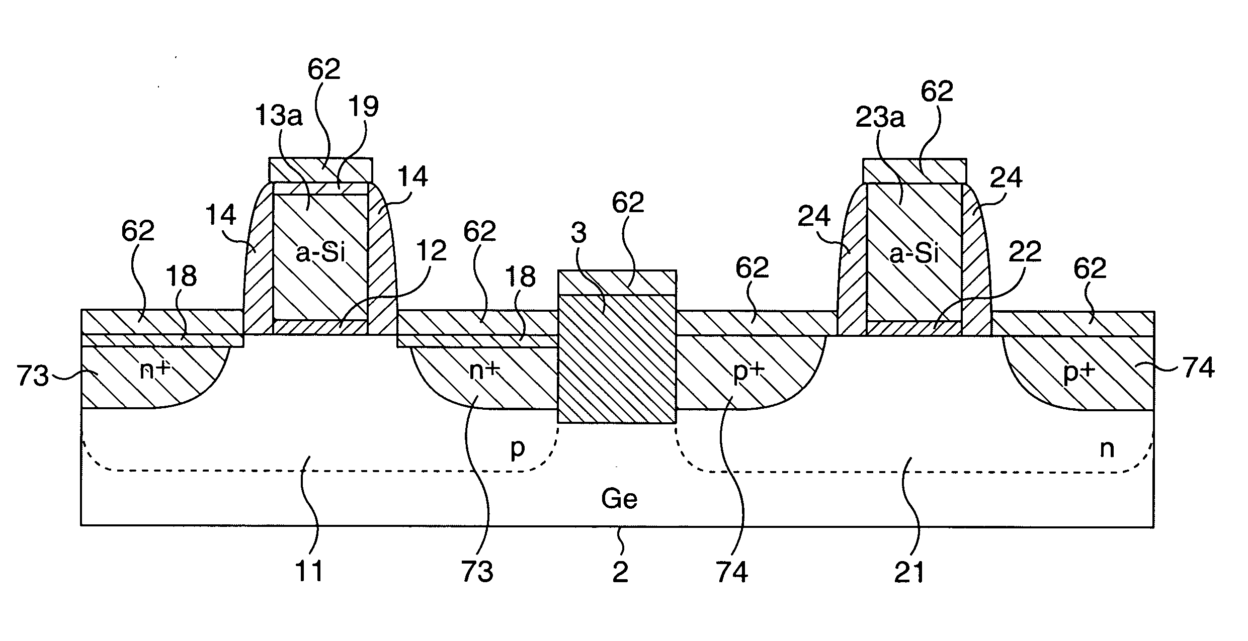
[0120]In this embodiment, a method of manufacturing the Ge-channel CMOSFET shown in FIG. 3 will be described.
[0121]FIG. 11 to FIG. 14 are schematic cross-sectional views showing the method of manufacturing the Ge-channel CMOSFET according to the first embodiment, in order of processes.
[0122]First, as shown in FIG. 11, an STI 3 demarcating regions for forming the nMOSFET 10 and the pMOSFET 2 is formed on the Ge substrate 2. Then, a predetermined dose amount of an impurity of a predetermined conduction type is ion-implanted with a predetermined acceleration energy to each of the regions demarcated by the STI 3 and further the impurity is activated by heat treatment, whereby the p-well 11 and the n-well 21 are formed.
[0123]Subsequently, as shown in FIG. 12, a film of an insulative material such as GeON, SiO2, SiON, or a high-k insulative material is formed on the regions for forming the nMOSFET 10 and the pMOSFET 20, and thereafter amorphous Si is deposited thereon. A film of this amor...
second embodiment
[0144]Hereinafter, a second embodiment of the present invention will be described. A CMOSFET disclosed here is formed by using a GOI (Germanium On Insulator) substrate instead of the Ge substrate used in the first embodiment. For convenience of the description, the structure of the CMOSFET will be described along with a manufacturing method thereof.
[0145]FIG. 20 to FIG. 24 are schematic cross-sectional views showing major processes of the method of manufacturing the Ge-channel CMOSFET according to the second embodiment, in order of processes.
[0146]A GOI substrate 31 used here is structured such that a thin Ge layer 31c is formed on a support substrate 31a such as a Si substrate via an insulation film 31b of SiO2 or the like. The GOI substrate 31 can be formed by, for example, a so-called oxidation and condensation method or the like which oxidizes a SiGe layer formed on a SOI (Silicon On Insulator) substrate to increase a Ge composition. Incidentally, a thickness of the Ge layer 31c...
modified example
[0158]Here, a modified example of the second embodiment will be described. The same reference numerals and symbols are used here to designate the same constituent members and so on as those described in the first embodiment.
[0159]FIG. 25 to FIG. 27 are schematic cross-sectional views showing major processes in a method of manufacturing a Ge-channel CMOSFET according to the modified example of the second embodiment, in order of processes.
[0160]First, after a STI 32 is formed on an about 30 nm Ge layer 31c of a GOI substrate 31 and ion-implantation for threshold voltage adjustment is performed as shown in FIG. 20, gate insulation films 41, 51, gate electrodes 42, 52, and sidewalls 43, 53 are formed as shown in FIG. 21.
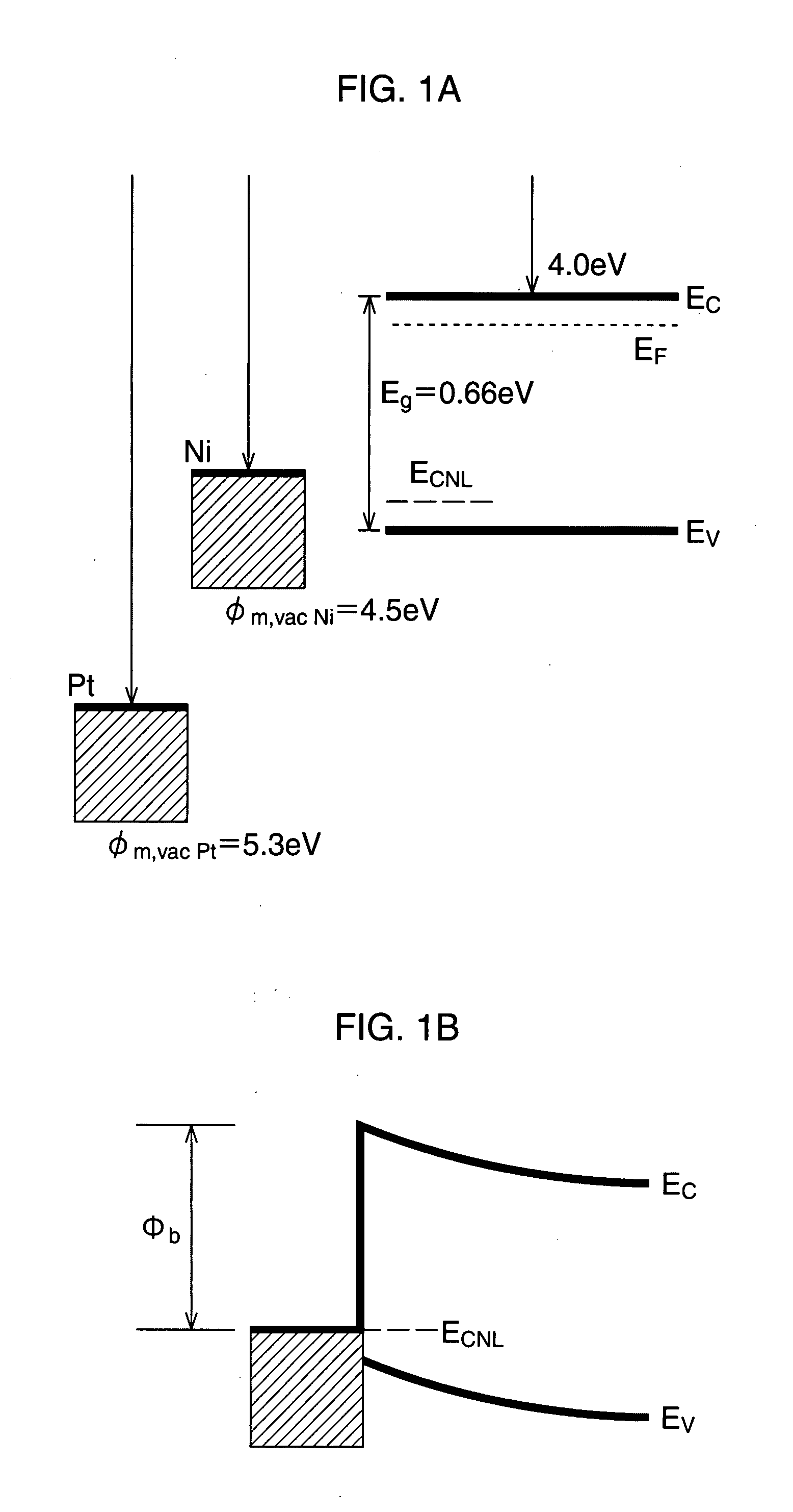
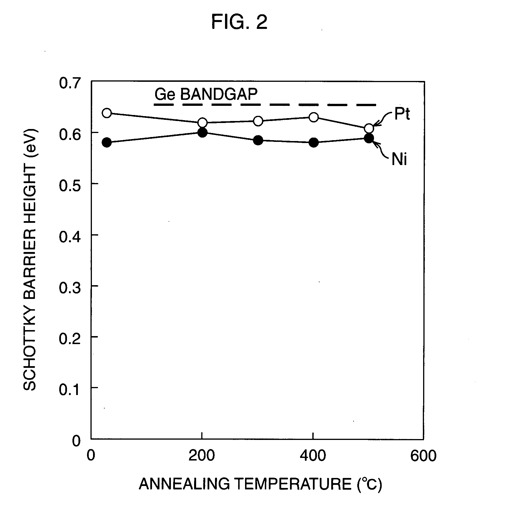
[0161]Then, after a Ni film 64 with a thickness of about 15 nm is deposited on the whole surface as shown in FIG. 25, RTA is performed at a temperature within the proper temperature range described in the second embodiment for a predetermined time as shown in FIG. 26. Co...
PUM
 Abstract
Description
Claims
Application Information