

System for magnetic scanning and correction of an ion beam
- Summary
- Abstract
- Description
- Claims
- Application Information
AI Technical Summary
Benefits of technology
Problems solved by technology
Method used
Image

Examples
Embodiment Construction
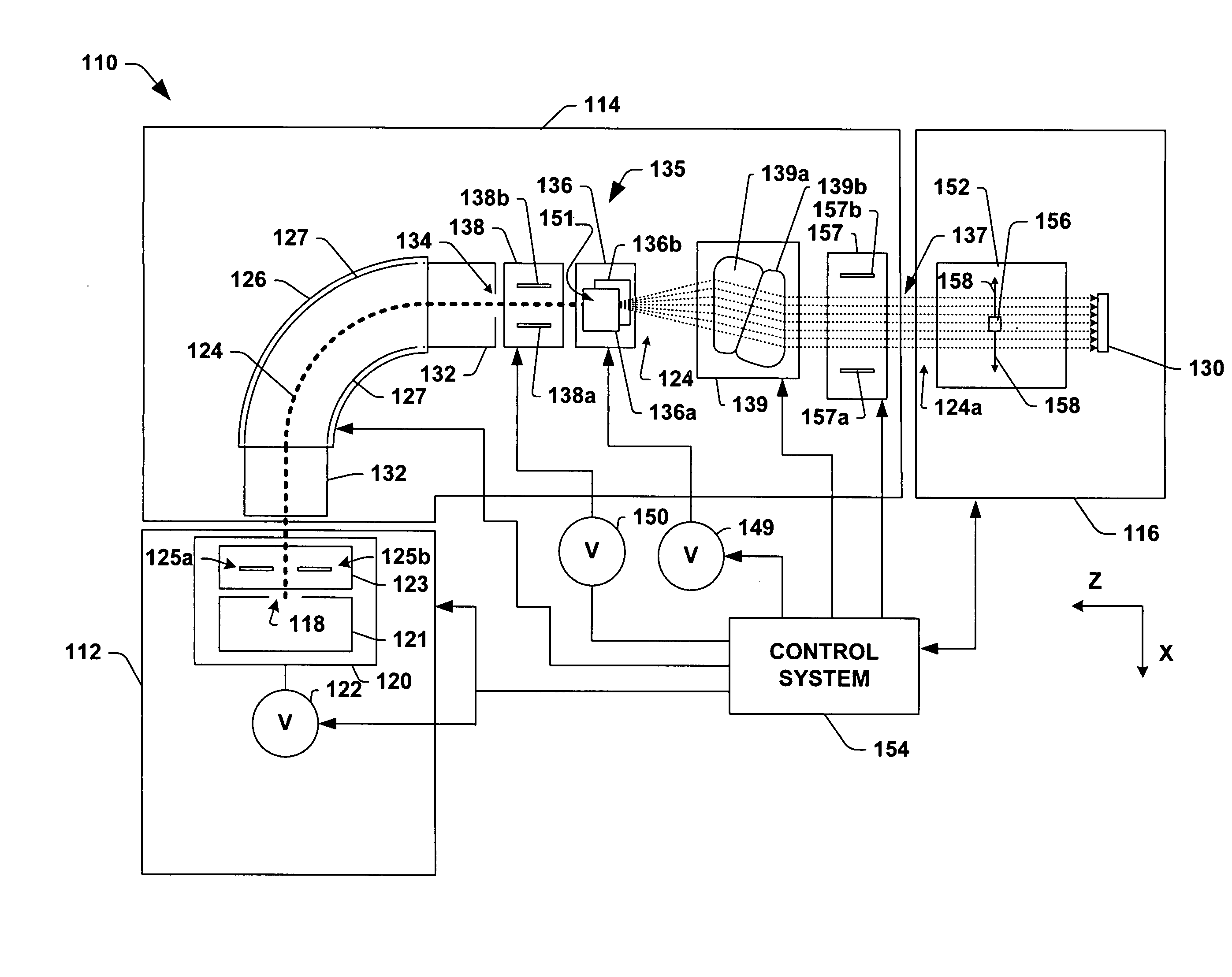
[0022]The present invention will now be described with reference to the drawings wherein like reference numerals are used to refer to like elements throughout, and wherein the illustrated structures are not necessarily drawn to scale.
[0023]Aspects of the present invention facilitate ion implantation by mitigating the zero field effect, which typically occurs in magnetic based scanners during time periods of zero or about zero magnetic field amplitudes. A constant magnetic field is applied to an ion beam near or within the magnetic scanner in order to mitigate the zero field effect and smooth the flux profile.
[0024]FIG. 1 illustrates an example ion implantation system 110 in accordance with an aspect of the present invention. The system 110 is presented for illustrative purposes and it is appreciated that aspects of the invention are not limited to the described ion implantation system and that other suitable ion implantation systems can also be employed.
[0025]The system 110 has a te...
PUM
 Abstract
Description
Claims
Application Information