Micropipe-free silicon carbide and related method of manufacture

a technology of silicon carbide and micropipes, which is applied in the direction of water-setting substance layered products, crystal growth processes, transportation and packaging, etc., can solve the problems of limiting the broader use of sic wafers, affecting device yield and reliability, and structural defects causing the effect of fabrication damag

Active Publication Date: 2008-03-20
CREE INC
View PDF19 Cites 22 Cited by
  • Summary
  • Abstract
  • Description
  • Claims
  • Application Information

AI Technical Summary

Benefits of technology

[0015] In one embodiment, the invention provides a method of growing a single-crystal of silicon carbide (SiC crystal) in the nominal c-axis growth direction using a physical vapor transport (PVT) process in a sublimation system, wherein the crystal is completely free of micropipe defects, the method comprising; attaching a seed material to a seed holder and forming a uniform thermal contact between the seed material and seed holder, placing a source material and the seed material attached to the seed holder in a reaction crucible, wherein constituent components of the sublimation system including at least the source material, the seed holder, and the reaction crucible are substantially free from unintentional impurities, and controlling growth temperature, growth pressure, SiC sublimation flux and composition, and a temperature gradient between the source material and the seed material or the SiC crystal growin

Problems solved by technology

However, certain materials-related problems continue to impede the broader use of SiC wafers as the substrate of choice in many commercial applications.
These materials-related problems are largely the result of certain structural defects in the material composition of conventionally manufactured SiC, such as micropipes, dislocations (e.g., threading, edge, basal plane, and/or screw dislocations), hexagonal voids, stacking faults, etc.
Such structural defects are detrimental to fabrication and proper operation of semiconductor devices subsequently formed on the SiC substrate.
Device yield

Method used


Image

  • Micropipe-free silicon carbide and related method of manufacture
  • Micropipe-free silicon carbide and related method of manufacture
  • Micropipe-free silicon carbide and related method of manufacture

Examples


Embodiment Construction

[0026] Embodiments of the invention will now be described in relation to the accompanying drawings. However, the invention is not limited to only the embodiments described herein. Rather, the selected embodiments are presented as teaching examples.

[0027] For purposes of clarity, certain embodiments of the invention are described in the context of known processes and related equipment. Those of ordinary skill in the art will recognize that the scope of the invention are not limited to only these processes and associated equipment. Rather, as SiC growth processes and associated equipment change and evolve over the succeeding years, the teachings of the present invention will find ready application within these new contexts.

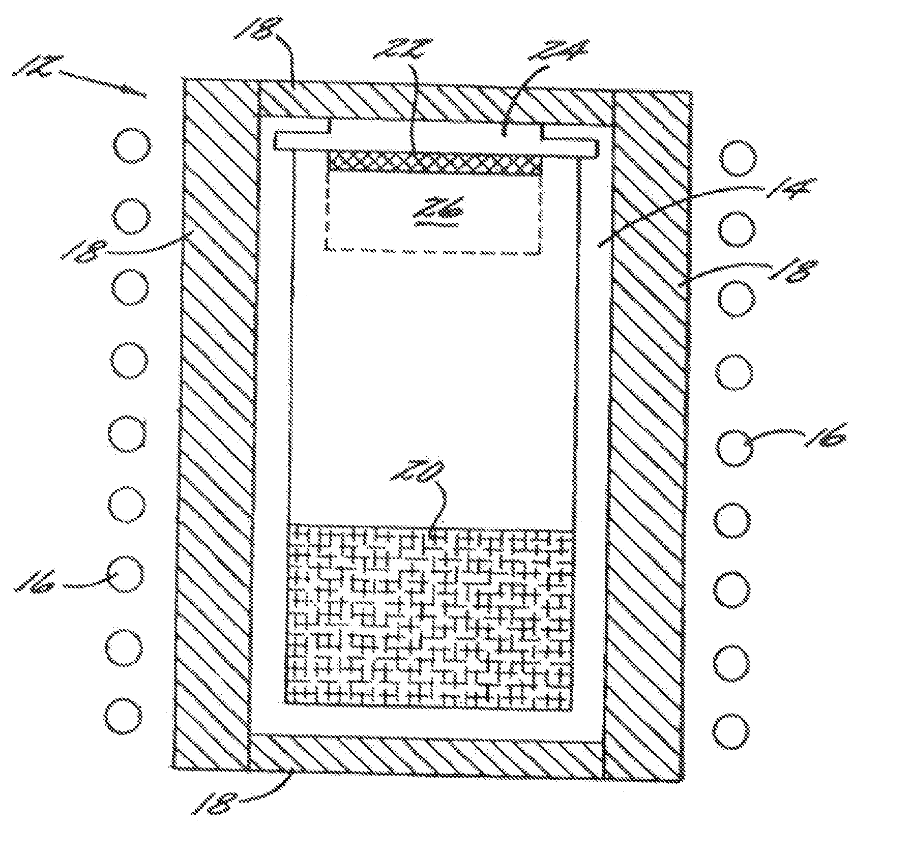
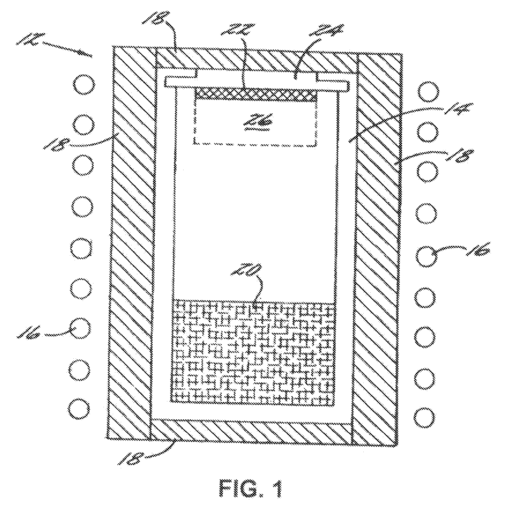
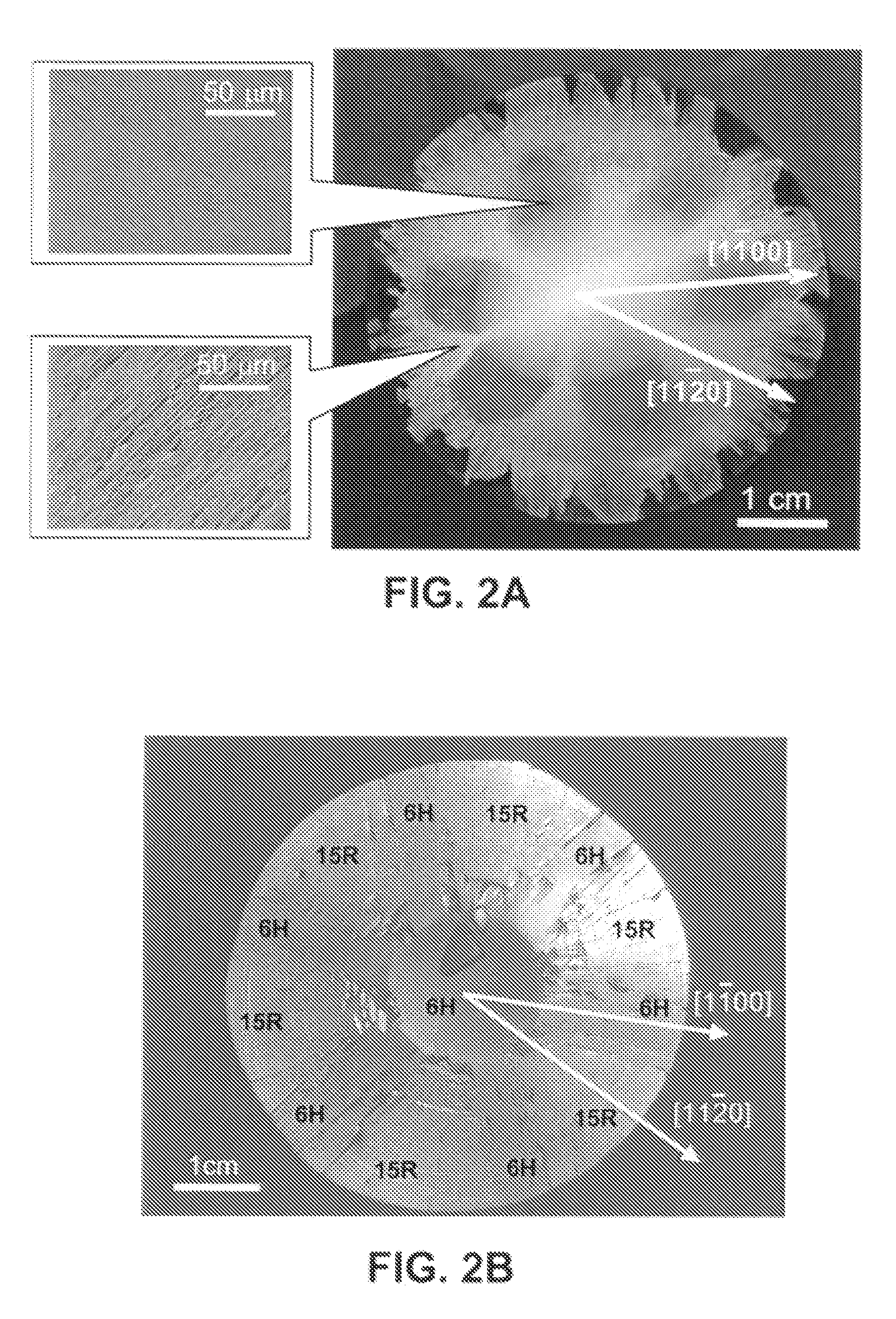
[0028] As is conventionally understood, a SiC boule may be grown using a seeded sublimation growth process, such as PVT, using a seeded sublimation system. Alternately, seeded sublimation systems may include high temperature CVD (HT-CVD) systems and halide CVD (H-...


PUM


Abstract

Micropipe-free, single crystal, silicon carbide (SiC) and related methods of manufacture are disclosed. The SiC is grown by placing a source material and seed material on a seed holder in a reaction crucible of the sublimation system, wherein constituent components of the sublimation system including the source material, reaction crucible, and seed holder are substantially free from unintentional impurities. By controlling growth temperature, growth pressure, SiC sublimation flux and composition, and a temperature gradient between the source material and the seed material or the SiC crystal growing on the seed material during the PVT process, micropipe-inducing process instabilities are eliminated and micropipe-free SiC crystal is grown on the seed material.

Description

[0001] This application claims the benefit of U.S. Provisional Application No. 60 / 844,360 filed on Sep. 14, 2006.BACKGROUND OF THE INVENTION [0002] 1. Field of the Invention [0003] The present invention relates to a micropipe-free silicon carbide, micropipe-free silicon carbide single crystal wafers, and related methods of manufacture. [0004] 2. Description of Related Art [0005] Single crystal silicon carbide (SiC) has proven to be a very useful material in the manufacture of various electronic devices. Due to its physical strength and excellent resistance to many chemicals, SiC may be used to fabricate very robust substrates adapted for use in the semiconductor industry. SiC has excellent electrical properties, including radiation hardness, high breakdown field, a relatively wide band gap, high saturated electron drift velocity, high-temperature operation, and absorption and emission of high-energy photons in the blue, violet, and ultraviolet regions of the optical spectrum. [0006]...

Claims


Application Information

Patent Timeline
IPC IPC(8): B32B3/00C01B31/00H01L29/94
CPCC30B29/36H01L21/02378H01L21/02433H01L21/02529H01L21/0254Y10T428/21H01L21/02634C30B23/002C30B23/005H01L29/1608H01L21/02631
Inventor BASCERI, CEMKHLEBNIKOV, YURIKHLEBNIKOV, IGORBALKAS, CENGIZSILAN, MURAT N.HOBGOOD, HUDSON MCD.CARTER, CALVIN H. JR.BALAKRISHNA, VIJAYLEONARD, ROBERT T.POWELL, ADRIAN R.TSVETKOV, VALERI T.JENNY, JASON R.
Owner CREE INC
Why Eureka
Try Eureka