Damascene Contact Structure for Integrated Circuits

Active Publication Date: 2008-03-27
CHARTERED SEMICONDUCTOR MANUFACTURING
View PDF20 Cites 48 Cited by
  • Summary
  • Abstract
  • Description
  • Claims
  • Application Information

AI Technical Summary

Benefits of technology

[0007]In yet another aspect of the invention, a method for forming interconnections is disclosed. The method comprises forming an interconnecting barrier which lines a cavity disposed on a substrate. A liner layer is then formed on the substrate over the interconnecting barrier followed by filling the cavity with a c

Problems solved by technology

However, designers are faced with numerous challenges regarding interconnections as technology progresses beyond deep ultraviolet (DUV) lithography (<193 nm).
Striations can result in shorts as well as other problems.
Additionally, due to the softer photoresist being used, a larger photoresist budget or thicker photoresist

Method used


Image

  • Damascene Contact Structure for Integrated Circuits
  • Damascene Contact Structure for Integrated Circuits
  • Damascene Contact Structure for Integrated Circuits

Examples


Example

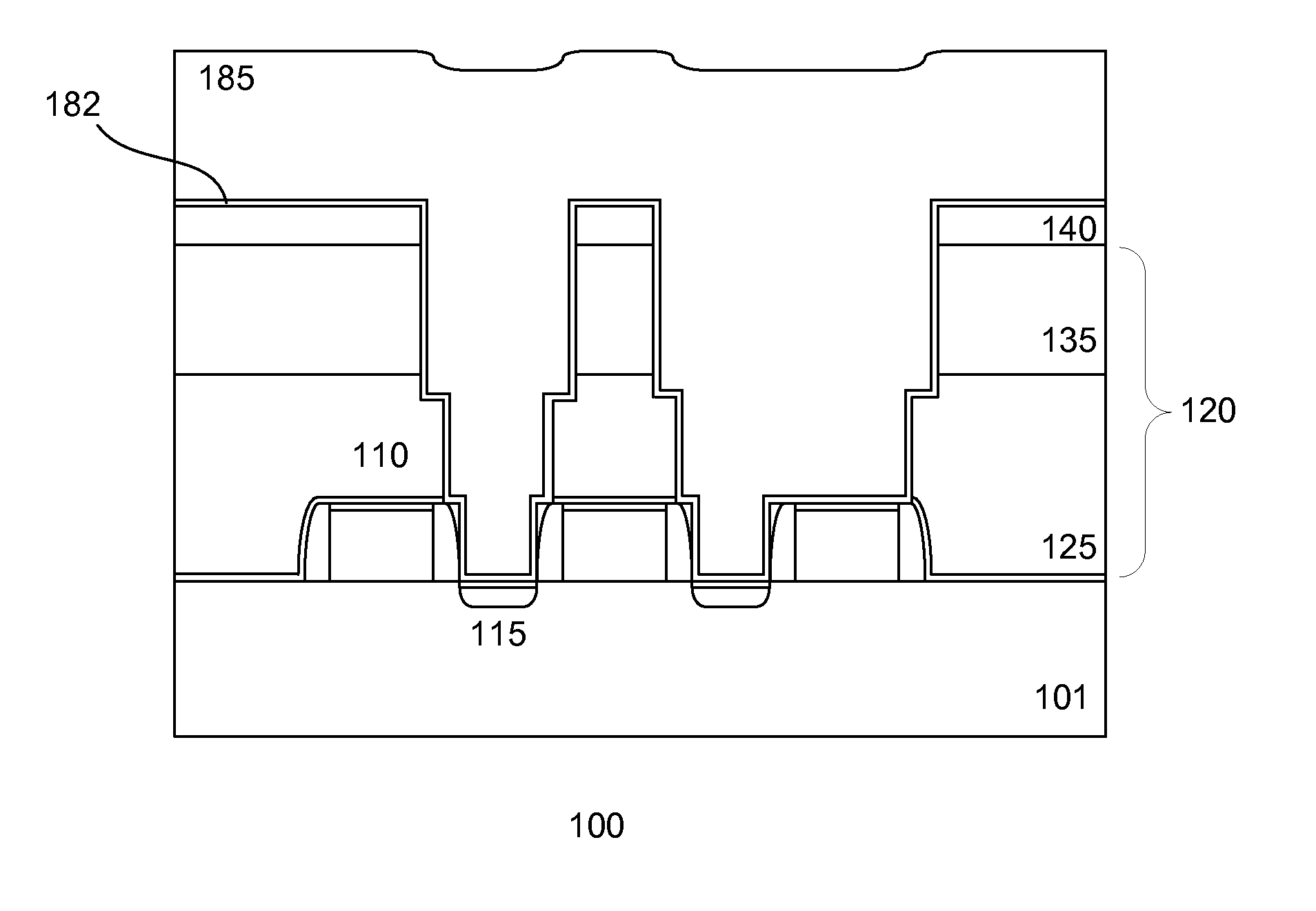
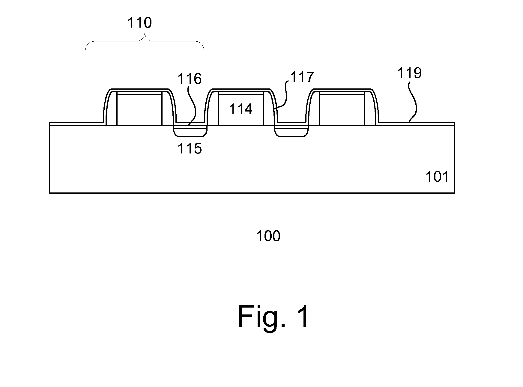
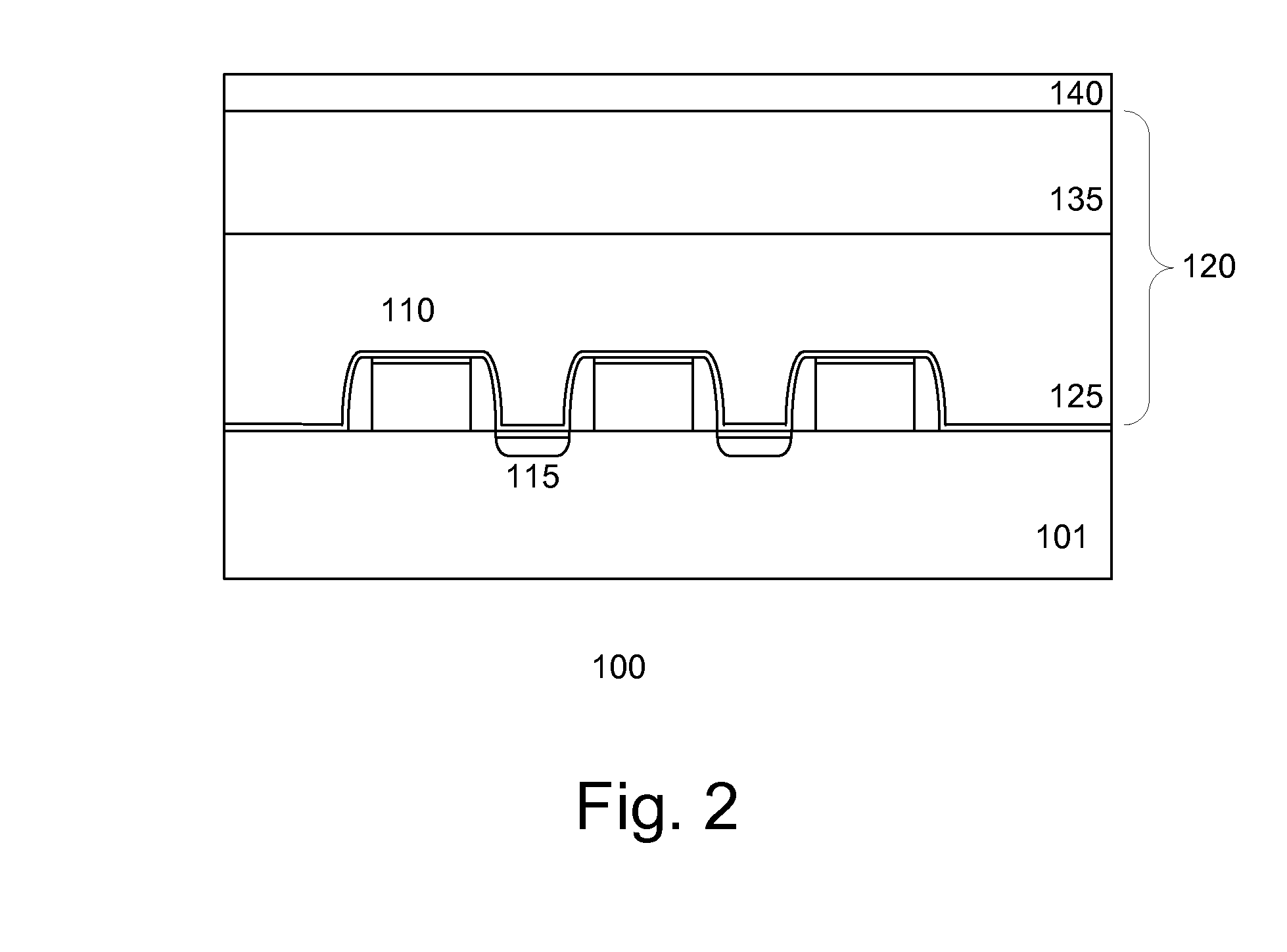
[0012]The present invention relates to ICs. More particularly, the present invention relates to interconnections and processes for forming such in ICs. The ICs can be any type of IC, for example dynamic or static random access memories, signal processors, or system on chip devices. In one embodiment, a damascene structure is formed using a hard mask layer. In one embodiment, the hard mask layer is used to form the lower and upper portions of the damascene structure. Alternatively, the hard mask layer can be used to form vias for contact plugs. The use of a hard mask layer reduces the photoresist budget, avoiding problems associated with thick photoresist layers. This increases the process window for forming interconnections which in turn raises yields and lowers manufacturing cost.

[0013]FIGS. 1-11 show a cross-sectional view of a portion of an integrated circuit (IC) 100 depicting a process for forming interconnections in accordance with one embodiment of the invention. Referring to...


PUM


Abstract

Interconnects for integrated circuits, such as damascene structures are formed using a hard mask. The hard mask is formed from, for example, high-k dielectric material such as hafnium oxide or other materials having high etch selectivity to the interconnect dielectric material. This enables a thin mask to etch vias and trenches in the interconnect dielectric layer, avoiding the problems associated with the use of thick mask layers, such as contact hole striations and small depth of focus, which can result in shorts or opens.

Description

FIELD OF THE INVENTION[0001]The present invention relates generally to integrated circuits, and more particularly damascene contacts in integrated circuits.BACKGROUND OF THE INVENTION[0002]The fabrication of integrated circuits (ICs) involves the formation of features on a substrate that make up circuit components, such as transistors, resistors and capacitors. The devices are interconnected, enabling the ICs to perform the desired functions. Interconnections are formed by forming contacts and conductive lines in an interconnecting dielectric layer (ICD) using, for example, damascene techniques. A damascene structure, for example, includes a via or contact hole in a lower portion and a trench which is generally wider than the contact hole in an upper portion. The via serves as a contact to a device while the trench contains the conductive line for connecting the device to, for example, other devices.[0003]To form the features and interconnections, layers are repeatedly deposited on ...

Claims


Application Information

Patent Timeline
IPC IPC(8): H01L21/44
CPCH01L21/31144H01L21/76846H01L21/76808H01L21/76895H01L21/76897H01L23/485H01L23/53238
Inventor YE, JIAN HUIZHOU, MEI SHENG
Owner CHARTERED SEMICONDUCTOR MANUFACTURING
Why Eureka
Try Eureka