Copper passivating post-chemical mechanical polishing cleaning composition and method of use

a technology of passivating post-chemical mechanical polishing and cleaning composition, which is applied in the preparation of detergent mixture compositions, cleaning using liquids, detergent compounding agents, etc., can solve the problems of reducing the efficiency of these processes for removing smaller sized particles, and affecting the cleaning effect of wet cleaning techniques

Inactive Publication Date: 2008-03-27
ADVANCED TECH MATERIALS INC
View PDF56 Cites 131 Cited by
  • Summary
  • Abstract
  • Description
  • Claims
  • Application Information

AI Technical Summary

Benefits of technology

[0016]One aspect of the invention relates to an alkaline aqueous cleaning composition, comprising at least one amine, at least one passivating agent, optionally at least one quaternary base, optionally at least one reducing agent, and water, wherein said alkaline aqueous cleaning composition is suitable for cleaning residue and contaminants from a microelectronic device having said residue and contaminants thereon. Optionally, the alkaline aqueous cleaning composition may further comprise at least one surfactant. Preferably, the alkaline aqueous cleaning composition comprises at least one reducing agent, and said reducing agent comprises ascorbic acid.
[0017]In another aspect, the present invention relates to a kit comprising, in one or more containers, one or more reagents for forming an alkaline aqueous cleaning composition, said one or more reagents selected from the group consisting of at least one amine, at least one passivating agent, optionally at least one quaternary base, optionally at least one reducing agent, and optionally water, and wherein the kit is adapted to form an alkaline aqueous cleaning composition suitable for cleaning material from a microelectronic device, wherein the material is selected from the group consisting of post-CMP residue, post-gas phase plasma etching residue, and contaminants thereof. Optionally, the alkaline aqueous cleaning compositions may further comprise at least one surfactant. Preferably, the alkaline aqueous cleaning composition comprises at least one reducing agent, and said reducing agent comprises ascorbic acid.
[0018]In yet another aspect, the present invention relates to a method of cleaning residue and contaminants from a microelectronic device having said residue and contaminants thereon, said method comprising contacting the microelectronic device with an alkaline aqueous cleaning composition for sufficient time to at least partially clean said residue and contaminants from the microelectronic device, wherein the alkaline aqueous cleaning composition includes at least one amine, at least one passivating agent, optionally at least one quaternary base, optionally at least one reducing agent, and water. Optionally, the alkaline aqueous cleaning compositions may further comprise at least one surfactant. Preferably, the alkaline aqueous cleaning composition comprises at least one reducing agent, and said reducing agent comprises ascorbic acid.
[0019]In a further aspect, the present invention relates to a method of manufacturing a microelectronic device, said method comprising contacting the microelectronic device with an alkaline aqueous cleaning composition for sufficient time to at least partially clean residue and contaminants from the microelectronic device having said residue and contaminants thereon, wherein the alkaline aqueous cleaning composition includes at least one amine, at least one passivating agent, optionally at least one reducing agent, optionally at least one surfactant, optionally at least one quaternary base, and water. Preferably, the alkaline aqueous cleaning composition comprises at least one reducing agent, and said reducing agent comprises ascorbic acid.
[0020]Yet another aspect of the invention relates to improved microelectronic devices, and products incorporating same, made using the methods of the invention comprising cleaning of residue and contaminants from the microelectronic device having said residue and contaminants thereon, using the methods and / or compositions described herein, and optionally, incorporating the microelectronic device into a product.
[0021]Other aspects, features and advantages of the invention will be more fully apparent from the ensuing disclosure and appended claims.

Problems solved by technology

In addition, the polishing of a copper / low dielectric constant material on a silicon wafer often generates carbon-rich particles that settle onto the wafer surface.
Conventional wet techniques use fluid flow over the wafer surface to remove contaminants and as such, their efficiency is limited by the thickness of the boundary layer created by the fluid flow.
Additional adhesion, due to chemical and hydrogen bonding, further complicates the cleaning capabilities of wet cleaning techniques and significantly reduces the efficiency of these processes for removing smaller sized contaminants.
Disadvantageously, some of the contaminants may be chemically inert to the chemical ingredients in the aqueous solution.
For example, carbon-rich particles or chemical reaction by-products attached to the wafer may not be easily removed by the chemicals in the aqueous cleaning solution.
However, it is still not sufficient to efficiently remove sub-0.3 μm sized particles from the wafer surface.
The use of low-k dielectric films such as carbon-doped oxides or organic films in dual damascene integration has added a further challenge to post-CMP cleaning in which only aqueous-based chemistries are used.
These films as well as CMP stop layers, such as silicon carbide, silicon nitride, and silicon oxynitride, are very hydrophobic and hence are difficult to clean with water-based cleaning solutions.
In addition, because the carbon atoms within most types of neutral-to-acidic slurries have a potential opposite to that of the copper surface, the carbon-rich particles are likely to attach to the copper surface, producing additional surface defects.
Post-gas phase plasma etch residues, which may include chemical elements present on the substrate and in the plasma gases, are typically deposited on the back end of the line (BEOL) structures and if not removed, may interfere with subsequent silicidation or contact formation.
Conventional cleaning chemistries often damage the ILD, absorb into the pores of the ILD thereby increasing the dielectric constant, and / or corrode the metal structures.
Disadvantageously, the preferred solvent, N,N′-dimethylacetamide (DMAC) has poor acceptance in the semiconductor industry because it extracts carbon from the ultra-low-k dielectric materials, increasing the dielectric constant of said dielectric material.
Another common problem in microelectronic device manufacturing is the film-like residue that remains on the semiconductor device substrate following CMP processing.
If not removed, these residues can cause damage to copper lines or severely roughen the copper metallization, as well as cause poor adhesion of layers applied subsequent to the post-CMP removal process.
Severe roughening of copper metallization is particularly problematic, since overly rough copper can cause poor electrical performance of the product semiconductor device.

Method used


Image

  • Copper passivating post-chemical mechanical polishing cleaning composition and method of use
  • Copper passivating post-chemical mechanical polishing cleaning composition and method of use
  • Copper passivating post-chemical mechanical polishing cleaning composition and method of use

Examples


example 1

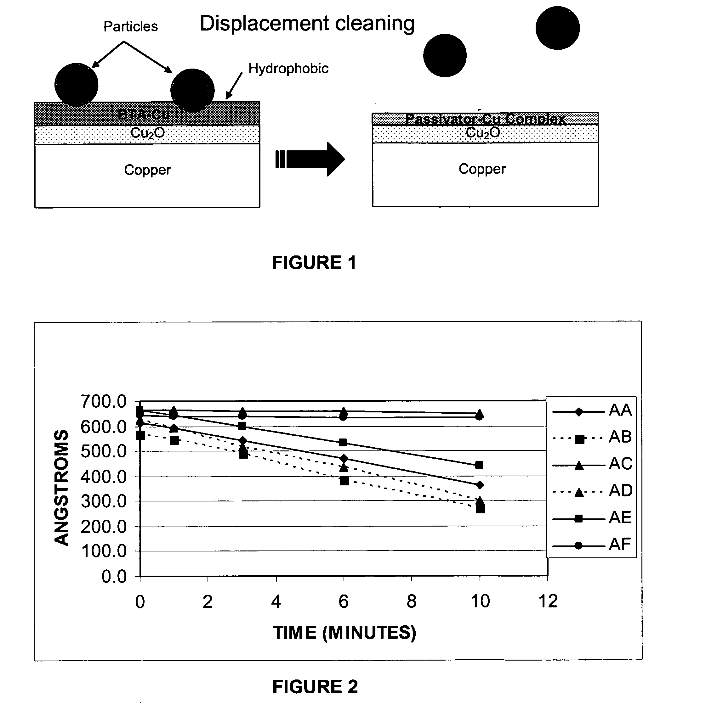
[0230]The efficacy of formulations AA-AF for inhibiting copper corrosion (i.e., minimizing copper etch rate) was evaluated. The device was a blanketed copper wafer. The wafer in each instance was immersed in the respective composition for 10 minutes at 50° C., followed by a deionized water rinse and spin dry. Prior to immersion, the samples were measured using the 4-point probe measurement technique to determine the thickness of the substrate as a function of resistivity. A regression curve was generated and the thickness of the copper determined as a function of resistivity to derive the etch rate of copper in each composition. The results are illustrated in FIG. 2.

example 2

[0231]A patterned wafer having residue thereon was immersed in a beaker of agitated (250 rpm) Formulation AC for 2 minutes at 40° C. The patterned wafer included a FSG bond pad on a copper surface. Subsequent to the clean, the wafer was rinsed with DI water, dried and submitted for scanning electron microscopy (SEM). The etch rate of copper was determined to be 1.4 Å min−1.

[0232]Electron micrographs of the control wafer before and after immersion are shown in FIGS. 3A and 3B, respectively. It can be seen that the residue was effectively removed following just 2 minutes of cleaning.

example 3

[0233]A post-via etch barrier break-through wafer was immersed in beaker of agitated (250 rpm) Formulation AC for 2 minutes at room temperature. During the via-etch process, the wafer was subjected to a 50% over etch to provide heavy sidewall polymer residue. Subsequent to the clean, the wafer was rinsed with DI water, dried and submitted for SEM.

[0234]Electron micrographs of the control via wafer and a cleaved control via wafer before immersion are shown in FIGS. 4A and 4B, respectively. Electron micrographs of the via wafer and the cleaved via wafer after immersion are shown in FIGS. 5A and 5B, respectively. It can clearly be seen that the residue remaining following the via etch and over-etch processes was substantially removed from the sidewalls of the vias (see, e.g., FIG. 5B).


PUM

PropertyMeasurementUnit
pHaaaaaaaaaa
pHaaaaaaaaaa
dielectric constantaaaaaaaaaa

Abstract

Alkaline aqueous cleaning compositions and processes for cleaning post-chemical mechanical polishing (CMP) residue, post-etch residue and/or contaminants from a microelectronic device having said residue and contaminants thereon. The alkaline aqueous cleaning compositions include amine, passivating agent, and water. The composition achieves highly efficacious cleaning of the residue and contaminant material from the microelectronic device while simultaneously passivating the metal interconnect material.

Description

FIELD OF THE INVENTION[0001]The present invention relates to alkaline aqueous compositions for cleaning post-chemical mechanical polishing (CMP) residue, post-etch residue and / or contaminants from microelectronic devices, wherein the aqueous cleaning compositions efficaciously remove post-CMP residue, post-etch residue and passivate metallic interconnect materials without damaging low-k dielectric material on the microelectronic device.DESCRIPTION OF THE RELATED ART[0002]As semiconductor device geometries continue to shrink to less than 0.18 μm, more emphasis has been placed on improved interconnect structures to minimize resistance-capacitance (RC) delays. Strategies to minimize interconnect delays include improving conductivity of the interconnect metal and lowering the dielectric constant (k) value of the dielectric layers. For example, copper has emerged as a replacement for conventional aluminum as the interconnect metal in advanced devices. Copper is more conductive than alumi...

Claims


Application Information

Patent Timeline
Patent Type & Authority Applications(United States)
IPC IPC(8): B08B7/00C11D7/32
CPCC11D3/0042H01L21/02074C11D3/28C11D3/30C11D3/34C11D7/265C11D7/32C11D7/3209C11D7/3218C11D7/3281C11D7/34C11D7/36C11D11/0047H01L21/02063C11D3/2079
Inventor BARNES, JEFFREY A.WALKER, ELIZABETHPETERS, DARRYL W.BARTOSH, KYLEOLDAK, EWA R.YANDERS, KEVIN P.
Owner ADVANCED TECH MATERIALS INC
Why Eureka
Try Eureka