Electrically pumped low-threshold ultra-small photonic crystal lasers

a photonic crystal laser and ultra-small technology, applied in the field of lasers and detectors, can solve the problems of large surface recombination loss, light re-absorption loss, and observed photonic crystal laser cavities, and achieve the effects of avoiding surface recombination loss, large strain gradient, and high band gap

Inactive Publication Date: 2008-04-03
CALIFORNIA INST OF TECH
View PDF6 Cites 15 Cited by
  • Summary
  • Abstract
  • Description
  • Claims
  • Application Information

AI Technical Summary

Benefits of technology

[0009] The invention generally relates to laser and detector devices that can comprise a photonic crystal. Using a laser as an example, the light emitting material in the laser is deliberately grown to experience a large strain. As the laser is microfabricated, this strain is relaxed on the newly etched surfaces, resulting in a large strain gradient between the unpatterned regions and the etched regions. This strain gradient gives rise to changes in the bandgap of the semiconductor quantum wells, and can be used for preventing electrons and holes from reaching the surface and avoiding surface recombination losses, rendering the quantum well material close to the etched surfaces to have a higher bandgap than the material a

Problems solved by technology

A number of problems in photonic crystal laser cavities have been observed.
These problems are related to the unique geometry of photonic crystal lasers, which require small features to be etched through active material to define mirrors and cavities lithographically.
The small dimensions of the etched features leads to potentially large surface recombination losses.
Moreover the same material that generates light in optical cavities also constitutes the etched regions that reflect the light, resulting in

Method used


Image

  • Electrically pumped low-threshold ultra-small photonic crystal lasers
  • Electrically pumped low-threshold ultra-small photonic crystal lasers
  • Electrically pumped low-threshold ultra-small photonic crystal lasers

Examples


Embodiment Construction

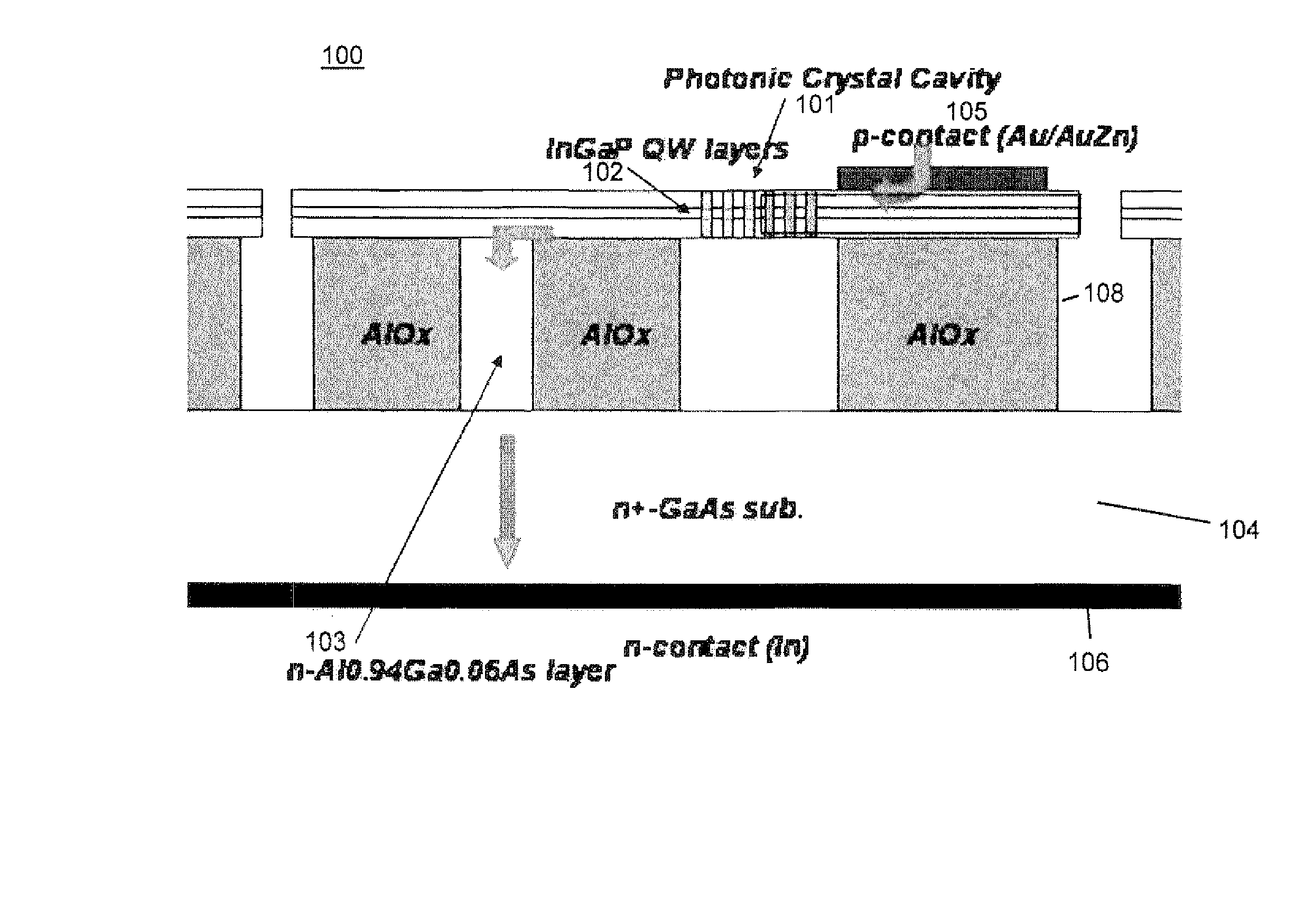
[0035] Our photonic crystal laser design addresses traditional problems that have been encountered in photonic crystal lasers emitting at longer wavelengths by (a) avoiding Auger recombination through the use of high-bandgap light emitting quantum wells, (b) avoiding surface recombination through the use of strain confinement of carriers to within the laser cavity and (c) avoiding re-absorption of light by deliberately engineering differences in strain into the quantum wells within the cavity compared to the photonic crystal mirrors surrounding the cavity. FIG. 1 is a cross sectional diagram that shows one exemplary embodiment of a photonic crystal laser 100 according to the invention. The embodiment of FIG. 1 is an illustrative electrically pumped photonic crystal design where a laterally defined p-n junction excites quantum well emission in the photonic crystal, Photonic crystal cavity 101 includes InGaP QW layers 102. Photonic crystal cavity 101 can be supported by one or more al...


PUM


Abstract

The invention is a photonic crystal laser including a photonic crystal slab laser cavity including InGaP/InGaAlP crystalline layers, the InGaP/InGaAlP crystalline layers having a relaxed strain at one or more etched surfaces and a higher strain at a plurality of quantum wells and at a distance from the one or more etched surfaces. The photonic crystal laser also includes electrical pads configured to receive an electrical signal the electrical pads attached to the photonic crystal slab laser cavity via an insulating layer, the photonic crystal laser configured to emit a laser light in response to the electrical signal. In another aspect, the invention features a photonic crystal detector including a photonic crystal slab cavity including InGaP/InGaAlP crystalline layers. In yet another aspect, the invention features a process to fabricate a photonic crystal laser cavity.

Description

CROSS-REFERENCE TO RELATED APPLICATIONS [0001] This application claims priority to and the benefit of co-pending U.S. provisional patent application Ser. No. 60 / 830,750, filed Jul. 13, 2006, which application is incorporated herein by reference in its entirety.STATEMENT REGARDING FEDERALLY FUNDED RESEARCH OR DEVELOPMENT [0002] The U.S. Government has certain rights in this invention pursuant to Grant No F49620-03-1-0418 awarded by the Air Force Office of Scientific Research (AFOSR).FIELD OF THE INVENTION [0003] The invention relates to lasers and detectors in general and particularly to a laser or detector that employs a photonic crystal laser cavity. BACKGROUND OF THE INVENTION [0004] A number of problems in photonic crystal laser cavities have been observed. These problems are related to the unique geometry of photonic crystal lasers, which require small features to be etched through active material to define mirrors and cavities lithographically. The small dimensions of the etche...

Claims


Application Information

Patent Timeline
IPC IPC(8): H01S5/34H01L21/00H01S5/185
CPCB82Y20/00H01S5/0207H01S5/0218H01S5/041H01S5/0425H01S5/10H01S5/423H01S5/18H01S5/183H01S5/2045H01S5/34326H01S5/4087H01S5/105H01S5/04256H01S5/11H01S5/185
Inventor SCHERER, AXEL
Owner CALIFORNIA INST OF TECH
Why Eureka
Try Eureka