Manufacturing method of semiconductor device

a manufacturing method and semiconductor technology, applied in semiconductor devices, semiconductor/solid-state device details, electrical devices, etc., can solve the problems of increasing the number of required masks, difficulty in cost reduction, complex processing procedures, etc., and achieve the effect of reducing the number of masks and the number of process steps

Active Publication Date: 2008-04-03
HEFEI RELIANCE MEMORY LTD
View PDF6 Cites 86 Cited by
  • Summary
  • Abstract
  • Description
  • Claims
  • Application Information

AI Technical Summary

Benefits of technology

[0024]According to the present invention, the use of a solution capable of dissolving cobalt but not tungsten makes it possible to form a plurality of contact holes reaching the metal

Problems solved by technology

This makes the processing procedures complicated and increases the numbe

Method used


Image

  • Manufacturing method of semiconductor device
  • Manufacturing method of semiconductor device
  • Manufacturing method of semiconductor device

Examples


Embodiment Construction

[0035]The present invention will be described with reference to the accompanying drawings.

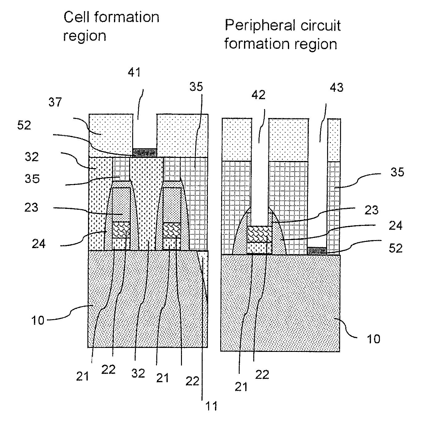
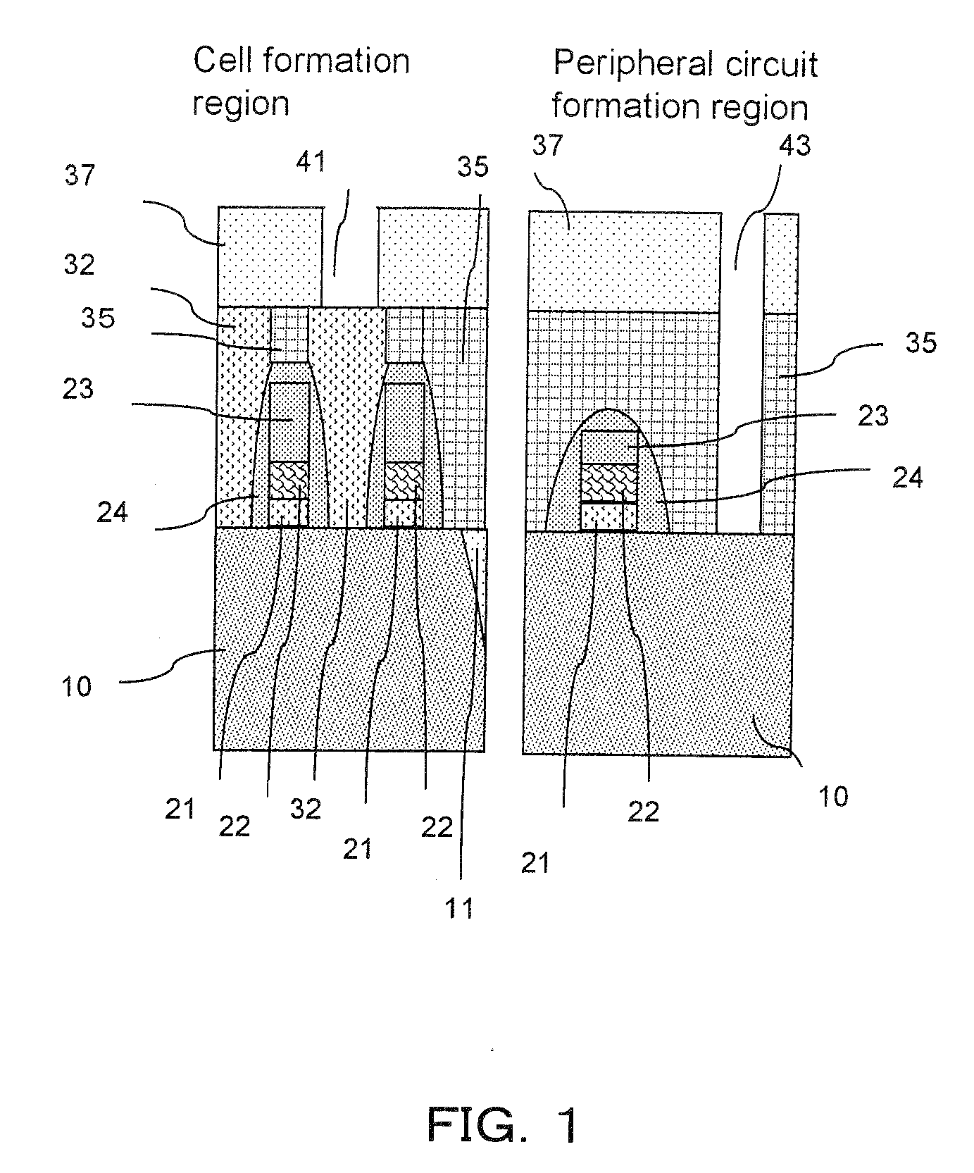
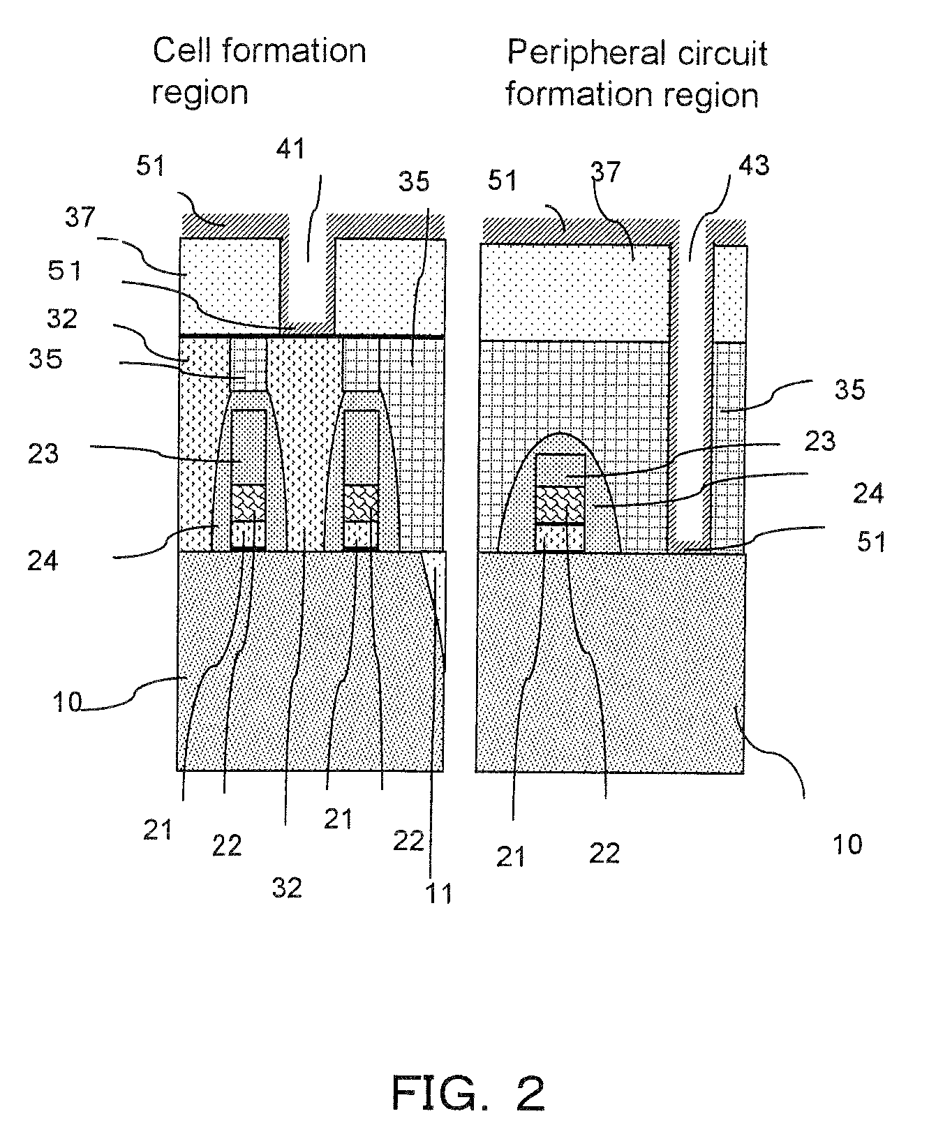
[0036]FIGS. 7 to 10 are cross-sectional views showing a exemplary embodiment of the present invention. These figures show part of a memory cell formation region (left side) and part of a peripheral circuit formation region (right) in respective steps of a DRAM device manufacturing process. Specifically, the left side of each of the drawings shows a region of a memory cell where a capacitance structure is formed later to store information. The right side shows a region to be a circuitry to control the read and write of information in the memory cell for each bit (for each “0” or “1” data).

[0037]FIG. 7 shows a structure, to which the exemplary embodiment is to be applied, and which has not been formed with openings yet. Prior to formation of the structure, a laminated structure is prepared which includes a gate insulating film (silicon oxide film) (not shown), a polysilicon film, tungsten nitride...


PUM


Abstract

A first structure is formed, having a contact plug formed on the bottom of a first opening in an interlayer insulating film, a second opening formed through the interlayer insulating film to reach a semiconductor substrate, and a third opening formed through the interlayer insulating film to reach a polymetal gate electrode. A cobalt layer is deposited on the surface of the structure, and thermally treated to form a cobalt silicide layer on the surface of the contact plug and on the bottom face of the second opening. The structure is then treated to remove the cobalt, in the state in which the cobalt silicide layer is formed, with the use of a chemical solution capable of dissolving cobalt but not the polymetal.

Description

[0001]This application is based upon and claims the benefit of priority from Japanese patent application No. 2006-264221 filed on Sep. 28, 2006, the disclosure of which is incorporated herein in its entirety by reference.BACKGROUND OF THE INVENTION[0002]1. Field of the Invention[0003]The present invention relates to a manufacturing method of a semiconductor device, and in particular to a resistance reduction process for a semiconductor device such as a DRAM device.[0004]2. Description of the Related Art[0005]In order to speed up a logic device or a device having DRAM and a logic circuit incorporated therein, it is necessary to reduce the resistance by a silicide process at the connection points where metal wiring is connected to a source electrode, drain electrode, gate electrode, and polysilicon contact. For this purpose, a cobalt silicide technology is typically utilized from the viewpoint of a wiring thinning effect or heat resistance (e.g. Japanese Laid-Open Patent Publication N...

Claims


Application Information

Patent Timeline
IPC IPC(8): H01L21/4763
CPCH01L21/02068H01L21/28518H01L21/32134H01L21/76814H01L21/76889H01L29/66545H01L27/10873H01L27/10888H01L27/10894H01L29/665H01L27/10855H10B12/0335H10B12/05H10B12/485H10B12/09
Inventor TANAKA, KENJI
Owner HEFEI RELIANCE MEMORY LTD
Why Eureka
Try Eureka