Semiconductor device and manufacturing method thereof

a technology of semiconductor devices and manufacturing methods, applied in the direction of semiconductor devices, basic electric elements, electrical appliances, etc., can solve the problems of adverse effects on threshold values, increase of equivalent silicon oxide thickness (eot) of gate insulators, other characteristics or reliability of mis transistors, etc., to enhance the reliability and characteristics of mis transistors, and reduce the mobility of mis transistors

Active Publication Date: 2008-04-10
RENESAS ELECTRONICS CORP
View PDF3 Cites 13 Cited by
  • Summary
  • Abstract
  • Description
  • Claims
  • Application Information

AI Technical Summary

Benefits of technology

[0018] As disclosed in Patent Document 2 (Japanese Patent Application Laid-Open Publication No. 2002-26317), when heated at high temperature of 800° C., a thick oxide film is formed at the upper and lower interface of gate insulator, and the EOT is increased, and also a nitrided region of high concentration is formed at the interface of silicon substrate and gate insulator, and mobility of MIS transistor is lowered.
[0019] As disclosed in Patent Document 3 (Japanese Patent Application Laid-Open Publication No. 2003-249649), when the gate insulator is nitrided after patterning the gate, a nitrided region of high concentration is formed in part of the interface of silicon substrate and gate insulator, and the mobility of MIS transistor is lowered.
[0020] It is hence an object of the present invention is to present a technology capable of enhancing the reliability and characteristics of the MIS transistor by using a gate insulator including a high-k film.

Problems solved by technology

As a result, if the MIS transistor is formed merely to be thinner, that is, by shortening the gate length only, the following problems are found.
That is, the presence of this oxide film 106 may lead to an increase of equivalent silicon oxide thickness (EOT) of the gate insulator 102, or may have adverse effects on the threshold value, other characteristics or reliability of MIS transistor.

Method used


Image

  • Semiconductor device and manufacturing method thereof
  • Semiconductor device and manufacturing method thereof
  • Semiconductor device and manufacturing method thereof

Examples


embodiment 1

[0048] As an example of a semiconductor device of the present invention, an Embodiment 1 relates to a semiconductor device having a MIS (Metal Insulator Semiconductor) transistor.

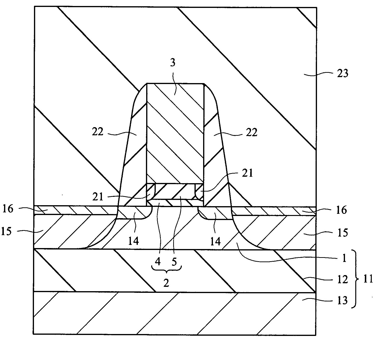
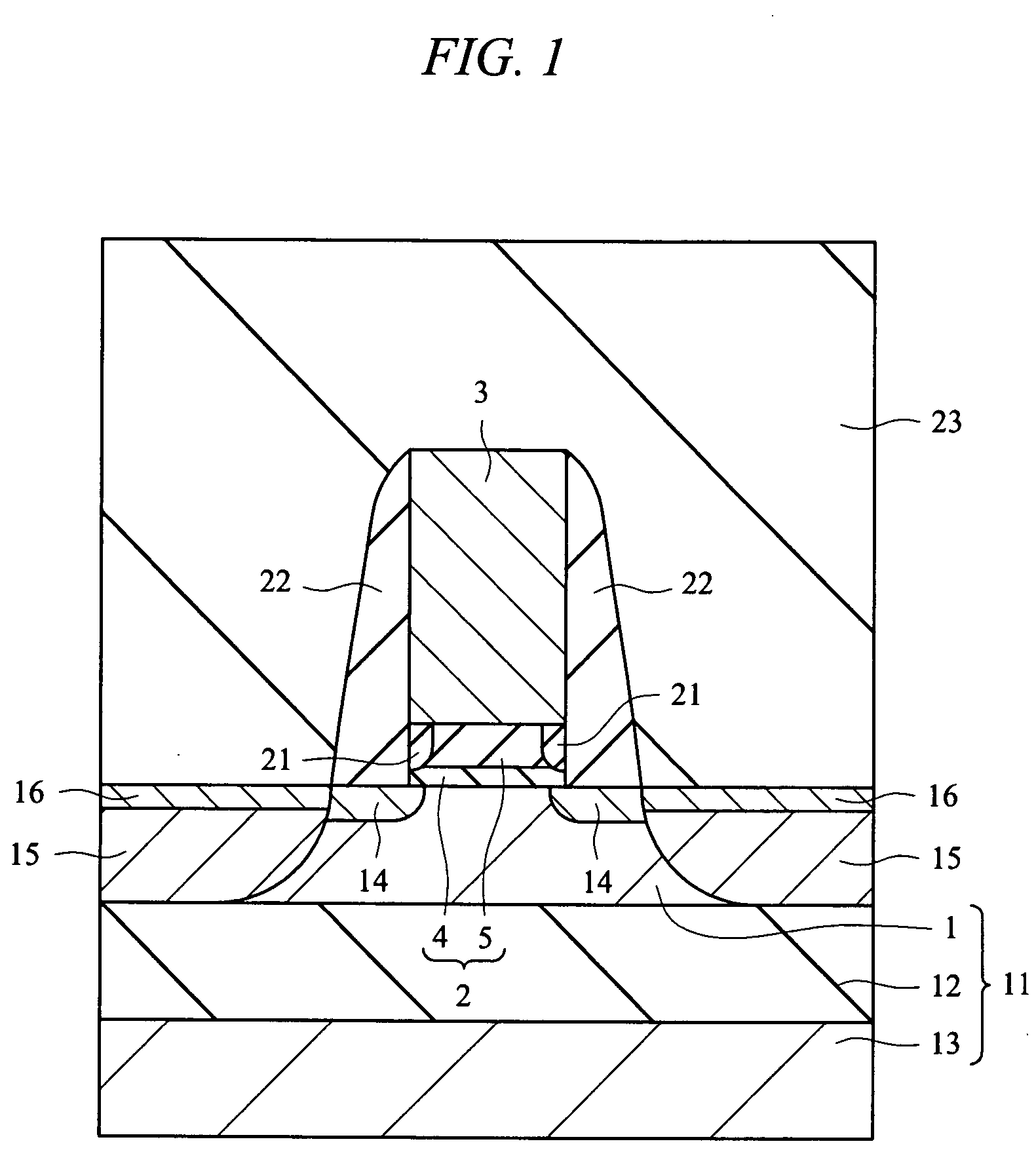
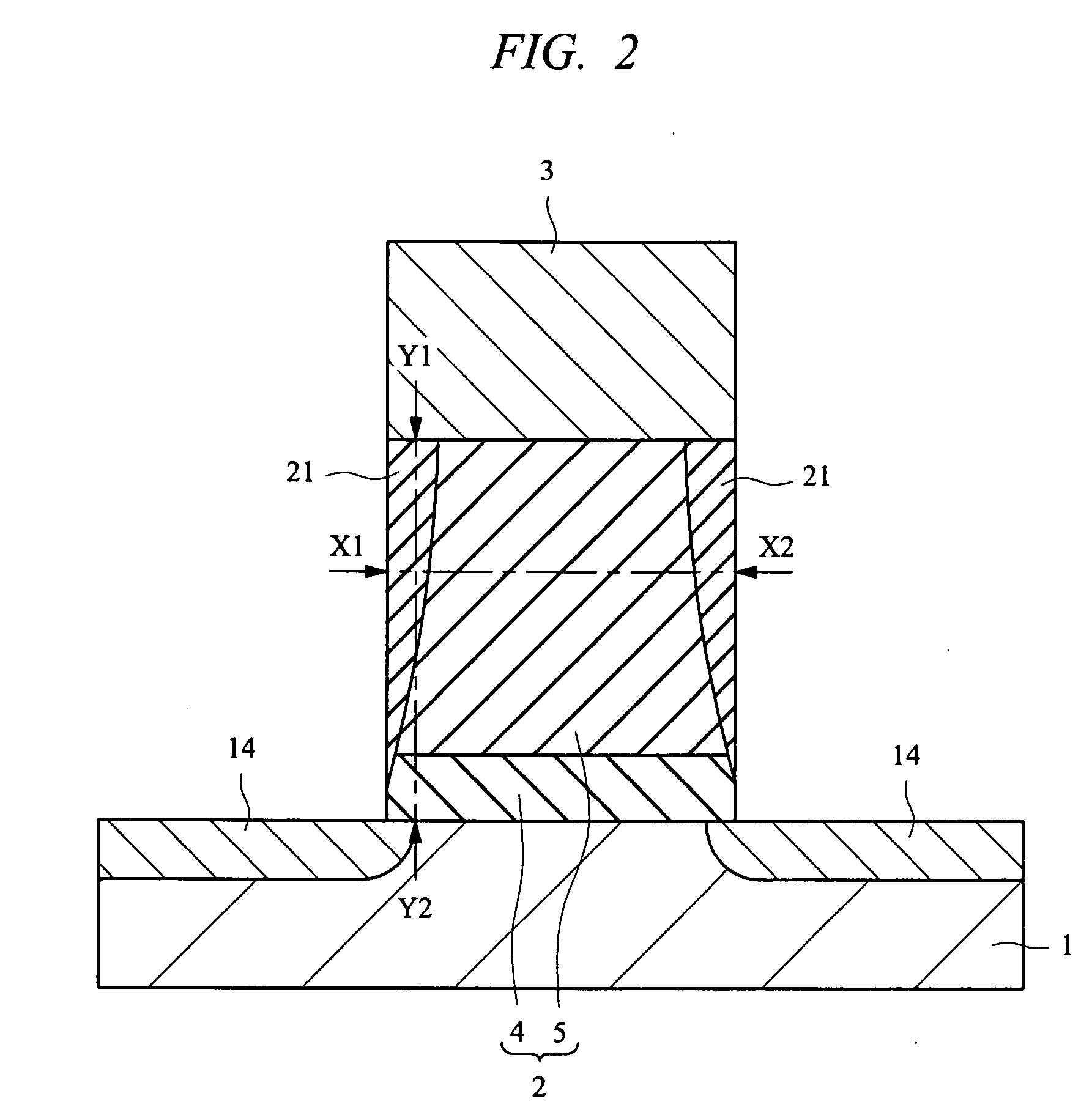
[0049]FIG. 1 is a schematic sectional view of main parts of a semiconductor device having a MIS transistor of the present Embodiment 1. FIG. 2 is a schematic enlarged sectional view of main parts of the MIS transistor in FIG. 1. As shown in FIG. 1 and FIG. 2, the MIS transistor has a MIS structure formed by an SOI (Silicon on Insulator) layer 1, a gate insulator 2, and a gate electrode 3. For example, the gate length of the MIS transistor is about 10 nm, the EOT of the gate insulator 2 is about 0.5 nm, and the thickness of SOI layer 1 is about 5 nm. In the Embodiment 1, the gate length is supposed to be about 10 nm, but it is applicable if the gate length is 10 nm or less.

[0050] The SOI layer 1 is an upper semiconductor layer isolated and separated from a lower supporting substrate 13 by means of a buried...

embodiment 2

[0077] As an example of a semiconductor device of the present invention, an Embodiment 2 relates to a semiconductor device having a MIS transistor.

[0078] The semiconductor device in the Embodiment 2 of the present invention differs from the semiconductor device having the MIS transistor described in the Embodiment 1 only in the material applied to the high-k film. That is, in the Embodiment 1, the high-k film is made of oxide containing hafnium (Hf) such as HfOx, HfAlOx or HfSiOx, but in the Embodiment 2, a rare earth oxide is used such as La2O3 or Y2O3.

[0079] The semiconductor device in the Embodiment 2 comprises, as shown in FIG. 1, a gate insulator 2 having a silicon oxide film 4 formed on the silicon substrate 11, and a high-k film 5 formed on the silicon oxide film 4, and this gate insulator 2 includes a nitrided region 21. That is, in the MIS transistor of the Embodiment 2, more nitrogen is contained at the lateral side than at the central side in gate length direction, and ...

embodiment 3

[0084] As an example of a semiconductor device of the present invention, an Embodiment 3 relates to a semiconductor device having a FinFET employing a Fin structure in the channel of a MIS transistor.

[0085] An example of a manufacturing method of semiconductor device in the Embodiment 3 is explained with reference to FIG. 13 to FIG. 17. FIG. 13 to FIG. 17 are schematic perspective views of main parts of the semiconductor device in the manufacturing process of the Embodiment 3.

[0086] First, a silicon substrate 61 having a supporting substrate 63, a buried oxide film 62, and an SOI layer 51 as shown in FIG. 13 is prepared.

[0087] Next, a Fin structure is processed as shown in FIG. 14. That is, the SOI layer 51 is etched selectively.

[0088] As shown in FIG. 15, further, to cover the SOI layer 51, a gate insulator 52 is deposited on the surface of the silicon substrate 61, and a polycrystalline silicon, a amorphous silicon, or a conductive film 53a is deposited on the gate film 52. Th...


PUM


Abstract

In a MIS transistor of which gate length is 10 nm or less, a gate insulator comprising a silicon oxide film formed on a silicon substrate and a high-k film formed on the silicon oxide film has a nitrided region including more nitrogen at the lateral side than at the central side in the gate-length direction, and including more nitrogen at the upper side than at the lower side in the film thickness direction. The reliability and characteristics of a MIS transistor using a gate insulator including a high-k (high dielectric constant) film is enhanced.

Description

CROSS-REFERENCE TO RELATED APPLICATION [0001] The present application claims priority from Japanese Patent Application No. JP 2006-27879 filed on Feb. 6, 2006, the content of which is hereby incorporated by reference into this application. TECHNICAL FIELD OF THE INVENTION [0002] The present invention relates to a semiconductor device and a manufacturing technique thereof. More particularly, the present invention relates to a technique effectively applied to a semiconductor device having a MIS (Metal Insulator Semiconductor) transistor using a gate insulator including a high-k film (high dielectric constant film). BACKGROUND OF THE INVENTION [0003] Recently, as MIS transistors which form semiconductor integrated circuits have been scaled, gate insulator thereof has become rapidly thinner. Consequently, influences of depletion in the gate electrode (polycrystalline silicon film) near the interfaces between the gate electrode and gate insulator caused when gate voltage is applied to a ...

Claims


Application Information

Patent Timeline
Patent Type & Authority Applications(United States)
IPC IPC(8): H01L29/76H01L21/336
CPCH01L21/28194H01L21/28202H01L29/495H01L29/4975H01L29/512H01L29/785H01L29/517H01L29/518H01L29/66795H01L29/7833H01L29/513
Inventor MISE, NOBUYUKITORIUMI, AKIRA
Owner RENESAS ELECTRONICS CORP
Why Eureka
Try Eureka