
Semiconductor polishing compound

a technology of semiconductors and polishing compounds, applied in lapping machines, other chemical processes, manufacturing tools, etc., can solve the problems of uneven surface (difference in level) in each layer of the production process, inability to planarize properly, and electrical performance tend to deteriorate, so as to achieve excellent dispersion stability and removal rate, and less susceptible to influence

Inactive Publication Date: 2008-04-17
ASAHI GLASS CO LTD +1
View PDF4 Cites 11 Cited by
  • Summary
  • Abstract
  • Description
  • Claims
  • Application Information

AI Technical Summary

Benefits of technology

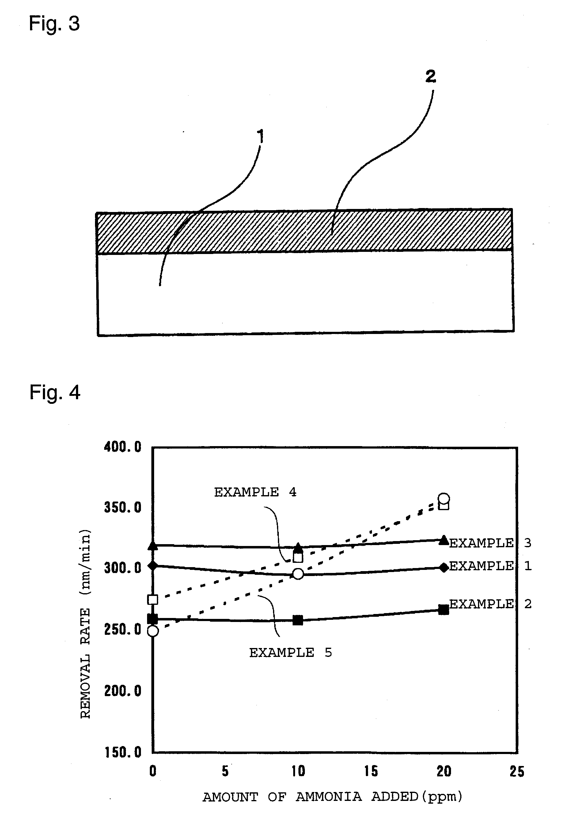
[0025] The semiconductor polishing compound of the present invention is not only excellent in dispersion stability and removal rate but also capable of exhibiting a stabilized polishing property, as it is less susceptible to an influence even when contacted with an alkaline polishing compound, particularly when contacted with ammonia evaporated from an alkaline polishing compound, in a multistage process.

Problems solved by technology

For example, as miniaturization of semiconductor integrated circuit devices and multilayered structures of wirings progresses, the surface unevenness (difference in level) in each layer in the production process tends to increase.
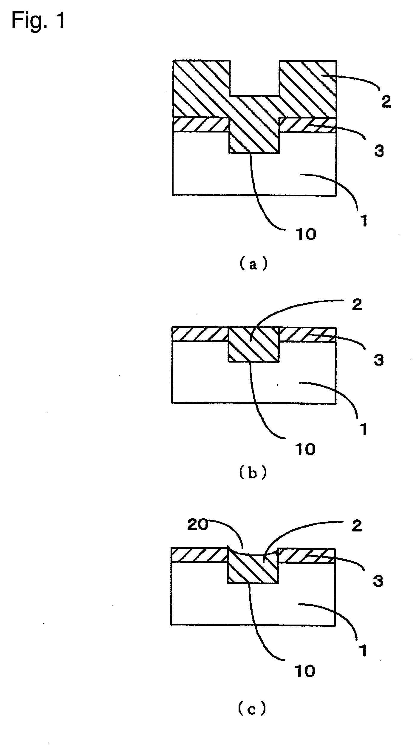
Here, if the polishing is excessive, the silicon dioxide film embedded in the trench 10 will be polished and recessed as shown in FIG. 1(c), whereby a structural defect such as a recess 20, so-called dishing, will result, and planarization tends to be inadequate or electrical performance tends to deteriorate.
However, if the concentration of the additive is increased, agglomeration of cerium oxide particles will be accelerated, whereby sedimentation of abrasive particles will result, and the dispersion stability of the polishing compound tends to deteriorate.
Further, if agglomeration of particles takes place, scratches will increase, thus leading to a problem that the integrated circuit device tends to be defective.
However, since the additive is at a high concentration, agglomeration of the abrasive particles is remarkable, and when the polishing solution is left to stand, cerium oxide abrasive particles will be completely sedimented within a few minutes.
In the polishing process of CMP, there is a waiting time during which no polishing is carried out, and sedimentation of abrasive particles is likely to result at a portion where the polishing compound is not always stirred or moved, thus causing clogging of the pipeline.
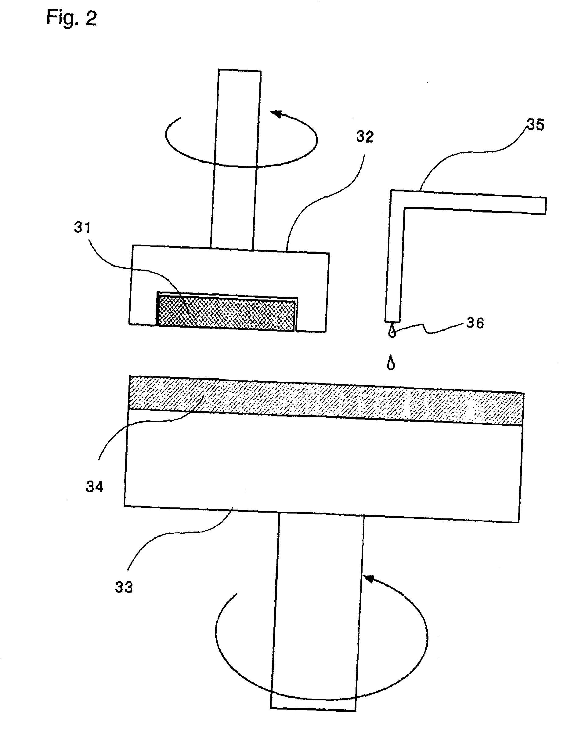
In order to prevent such sedimentation, there is a method of incorporating an additive to the polishing compound on a polishing pad or in a pipeline immediately before the polishing pad, but the mixing tends to be inadequate, the concentration tends to be non-uniform, or the polishing characteristics tend to be unstable.
Further, the abrasive particles on the pad tend to be agglomerated or deposited, whereby there has been a problem that scratches will increase.
Further, they have a serious problem that if an additive to improve the polishing property is incorporated excessively, agglomeration will be accelerated, whereby sedimentation by agglomeration tends to be remarkable.
Accordingly, the dispersibility of abrasive particles in the polishing compound was poor, and the abrasive particles were sedimented within a few minutes, whereby it was difficult to use such a polishing compound, and the removal rate was also inadequate.
However, with a polishing compound prepared in accordance with an Example wherein the concentration of the surfactant is lower, dishing fluctuation was substantial, and the planarization characteristic was poor.
Further, if the concentration of the surfactant becomes high, the number of scratches sharply increases.
Namely, it is considered that if coarse particles causing scratches, are present in abrasive particles even slightly, the particles will be agglomerated and accumulated on the polishing pad thereby to cause an increase of scratches.
Further, it is also considered that there may be a case where agglomerates of abrasive particles grown by agglomeration themselves will cause scratches.
As described in the foregoing, in the prior art, no polishing compound was available which had both dispersion stability of the polishing compound and excellent scratch characteristics, and excellent polishing planarization characteristics, and it was difficult to obtain a semiconductor integrated circuit device having adequate properties.
However, there has been a problem that by this method, cerium ions contained in the polishing compound will remain on a substrate and will present an adverse effect to the integrated circuit device.
However, in a case where CMP is carried out by a multistage process wherein the polishing compound of Patent Document 4 is used in combination with another alkaline compound (slurry), it has been likely that the pH changes by the influence of the alkaline polishing compound, which may adversely affect the polishing properties.

Method used


Image

  • Semiconductor polishing compound
  • Semiconductor polishing compound
  • Semiconductor polishing compound

Examples


example 1

[0087] Cerium oxide abrasive particles and, as an additive, an ammonium polyacrylate having a molecular weight of 5,000 were mixed in a mass ratio of 100:0.7 in deionized water with stirring, and subjected to ultrasonic dispersion and filtering to obtain a mixture having a concentration of abrasive particles of 10% by mass ratio and a concentration of the additive of 0.07%. This mixture was diluted five times with deionized water to prepare an abrasive particle mixed liquid A having an abrasive particle concentration of 2% and an additive concentration of 0.014%. The abrasive particle mixed liquid A had a pH of 7.6 and an average particle diameter of 0.18 μm.

[0088] Then, an ammonium polyacrylate having a molecular weight of 5,000 was dissolved in deionized water, and the pH adjustment was carried out by adding malonic acid (pKa2=5.28) to bring the pH to from 4.7 to 5.0, to prepare an additive liquid B having an ammonium polyacrylate concentration of 0.289% and a malonic acid concen...

example 2

[0090] An additive liquid C was prepared in the same manner as the preparation of the additive liquid B in Example 1 except that instead of malonic acid, adipic acid (pKa2=5.03) was used, and the concentration of adipic acid was adjusted to be 0.272%. This additive liquid C and the abrasive particle mixed liquid A prepared in the same manner as in Example 1 were mixed in a mass ratio of 1:1 with stirring to prepare a polishing compound having an abrasive particle concentration of 1%, an adipic acid concentration of 0.136% and a pH of 4.90.

example 3

[0091] An additive liquid D was prepared in the same manner as the preparation of the additive liquid B in Example 1 except that instead of malonic acid, succinic acid (pKa2=5.24) was used, and the concentration of succinic acid was adjusted to be 0.198%. This additive liquid D and the abrasive particle mixed liquid A prepared in the is same manner as in Example 1 were mixed in a mass ratio of 1:1 with stirring to obtain a polishing compound having an abrasive particle concentration of 1%, a succinic acid concentration of 0.099% and a pH of 5.06.


PUM

PropertyMeasurementUnit
Temperatureaaaaaaaaaa
Percent by massaaaaaaaaaa
Fractionaaaaaaaaaa

Abstract

To provide a semiconductor polishing compound which is excellent in dispersion stability and removal rate and which has a stabilized polishing property, as it is less susceptible to an influence even when contacted with an alkaline polishing compound during its application to CMP comprising a multistage process. A polishing compound for chemical mechanical polishing to polish a surface to be polished in the production of a semiconductor circuit device, said polishing compound comprising cerium oxide abrasive particles, water and a dicarboxylic acid represented by the formula 1: HOOC(CH2)nCOOH  Formula 1 wherein n is an integer of from 1 to 4, and the pH of said polishing compound at 25° C. being within a range of from 3.5 to 6.

Description

TECHNICAL FIELD [0001] The present invention relates to a semiconductor polishing compound for chemical mechanical polishing in a process for producing a semiconductor integrated circuit device. Particularly, it relates to a semiconductor polishing compound comprising cerium oxide, which is suitable for shallow trench isolation or planarization of an interlayer insulation film or a polysilicon. BACKGROUND ART [0002] In recent years, micro-fabrication techniques have been developed for miniaturization and high densification along with high integration and high functionality of semiconductor integrated circuit devices. Particularly, importance of planarization techniques by chemical mechanical polishing (hereinafter referred to as CMP) is increasing. [0003] For example, as miniaturization of semiconductor integrated circuit devices and multilayered structures of wirings progresses, the surface unevenness (difference in level) in each layer in the production process tends to increase. ...

Claims


Application Information

Patent Timeline
IPC IPC(8): B24D3/02B24B1/00B24B37/00C09K3/14H01L21/304
CPCC09G1/02H01L21/31053C09K3/1463C09K3/14
Inventor KON, YOSHINORIYOSHIDA, IORINAKAZAWA, NORIHITO
Owner ASAHI GLASS CO LTD
Learn More