Pulse plating of a low stress film on a solar cell substrate

a solar cell and substrate technology, applied in the field of pulse plating of low stress film on solar cell substrate, can solve the problems of loss of efficiency, discontinuous formation of grid electrode thin fingers, and increased resistive losses

a solar cell and substrate technology, applied in the field of pulse plating of low stress film on solar cell substrate, can solve the problems of loss of efficiency, discontinuous formation of grid electrode thin fingers, and increased resistive losses

US20080092947A1Inactive Publication Date: 2008-04-24APPLIED MATERIALS INC

Image

  • Pulse plating of a low stress film on a solar cell substrate
  • Pulse plating of a low stress film on a solar cell substrate
  • Pulse plating of a low stress film on a solar cell substrate

Examples


Embodiment Construction

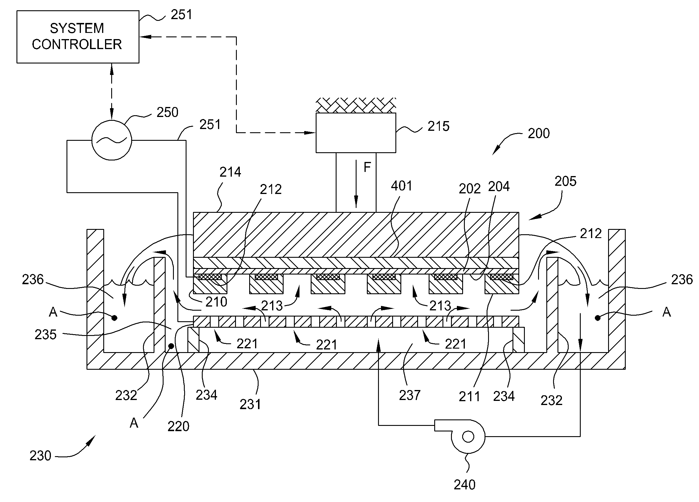
[0031]Embodiments of the invention contemplate the formation of a low cost solar cell metal contact structure that has improved electrical and mechanical properties by use of an electrochemical plating process. Solar cell substrates that may benefit from the invention include substrates composed of single crystal silicon, multi crystalline silicon, poly crystalline silicon, germanium (Ge), and gallium arsenide (GaAs), as well as heterojunction cells, such as GaInP / GaAs / Ge or ZnSe / GaAs / Ge substrates.

[0032]The resistance of interconnects formed in a solar cell device greatly affects the efficiency of the solar cell. It is thus desirable to form a solar cell device that has a low resistance connection that is reliable and cost effective. As noted above, silver (Ag) interconnecting lines formed from a silver paste is currently the preferred interconnecting method. However, while silver has a lower resistivity (e.g., 1.59×10⁻⁸ ohm-m) than other common metals such as copper (e.g., 1.7×10−...


PUM


Abstract

Embodiments of the invention contemplate the formation of a low cost solar cell metal contact structure that has improved electrical and mechanical properties through the use of an electrochemical plating process. The resistance of interconnects formed in a solar cell device greatly affects the efficiency of the solar cell. It is thus desirable to form a solar cell device that has a low resistance connections that is reliable and cost effective. One or more embodiments of the invention described herein are adapted to form a low cost and reliable interconnecting layer using an electrochemical plating process containing common metal, such as copper. However, generally the electroplated portions of the interconnecting layer may contain a substantially pure metal or a metal alloy layer. Methods are discussed herein that are used to form a solar cell containing conductive metal interconnect layer(s) that have a low intrinsic stress.

Description

BACKGROUND OF THE INVENTION[0001]1. Field of the Invention[0002]Embodiments of the present invention generally relate to the fabrication of photovoltaic cells and particularly to the formation of layers on a substrate by use of an electrochemical deposition process.[0003]2. Description of the Related Art[0004]Solar cells are photovoltaic devices that convert sunlight directly into electrical power. The most common solar cell material is silicon, which is in the form of single or polycrystalline wafers. Because the cost of forming a silicon-based solar cells is higher than the cost of generating electricity using traditional methods, there has been an effort to reduce the cost to form solar cells.[0005]FIGS. 1A and 1B schematically depicts a standard silicon wafer 100 fabricated on a wafer 110. The wafer 110 includes a p-type base region 101, an n-type emitter region 102, and a p-n junction region 103 disposed therebetween. An n-type region, or n-type semiconductor, is formed by dopi...

Claims


Application Information

Patent Timeline
24 Apr 2008
Publication
US20080092947A1
IPC
H01L31/00
CPC
Y02E10/50; H01L31/022425; H01L31/02245
Inventors
LOPATIN, SERGEY; GAY, CHARLES