Method for fixing plastic substrate, circuit substrate and method for producing same

Inactive Publication Date: 2008-05-01
FUJIFILM CORP
View PDF7 Cites 48 Cited by
  • Summary
  • Abstract
  • Description
  • Claims
  • Application Information

AI Technical Summary

Benefits of technology

[0030]In the invention, a plastic substrate is fixed by applying or sticking an adhesive material to a supporting substrate, and therefore, even a plastic substrate of which the strength and the toughness are poor by itself can be used in fabricating a thin-layer laminate device. In the invention, the adhesive strength in the peripheral part where a thin-film laminate device is not formed is high, and the center part where the device is formed is low, and therefore, a trouble of film delamination can be prevented throughout the process and the device can be smoothly cut out not detracting from the properties of the device. Fu

Problems solved by technology

However, when a glass substrate thinner than it is used, then it has a problem in that it may be readily cracked while produced or used.
However, because of various problems in that a plastic substrate is not rigid and is not tough, its thermal deformation temperature is low, its surface hardness is low and its surface is therefore readily scratched, and it readily undergoes deformation such as warping or thermal expansion or contraction in a heating step, the production of liquid-crystal display devices with such a plastic substrate is much more difficult than the production thereof with a glass substrate both in the case where the plastic substrate alone is conveyed by itself and in the case where the rolled plastic substrate is fed out.
However, in the production method where a plastic substrate is fixed in a frame and conveyed, the plastic substrate may be warped inside the frame and it could hardly keep its surface flatness.
Accordingly, in various units for the production of a liquid-crystal display device, there may be a problem in that an auxiliary member to assist the flatness of the frame insi

Method used


Image

  • Method for fixing plastic substrate, circuit substrate and method for producing same
  • Method for fixing plastic substrate, circuit substrate and method for producing same

Examples


Example

EXAMPLE 1

(A) Fixing Component Forming Step:

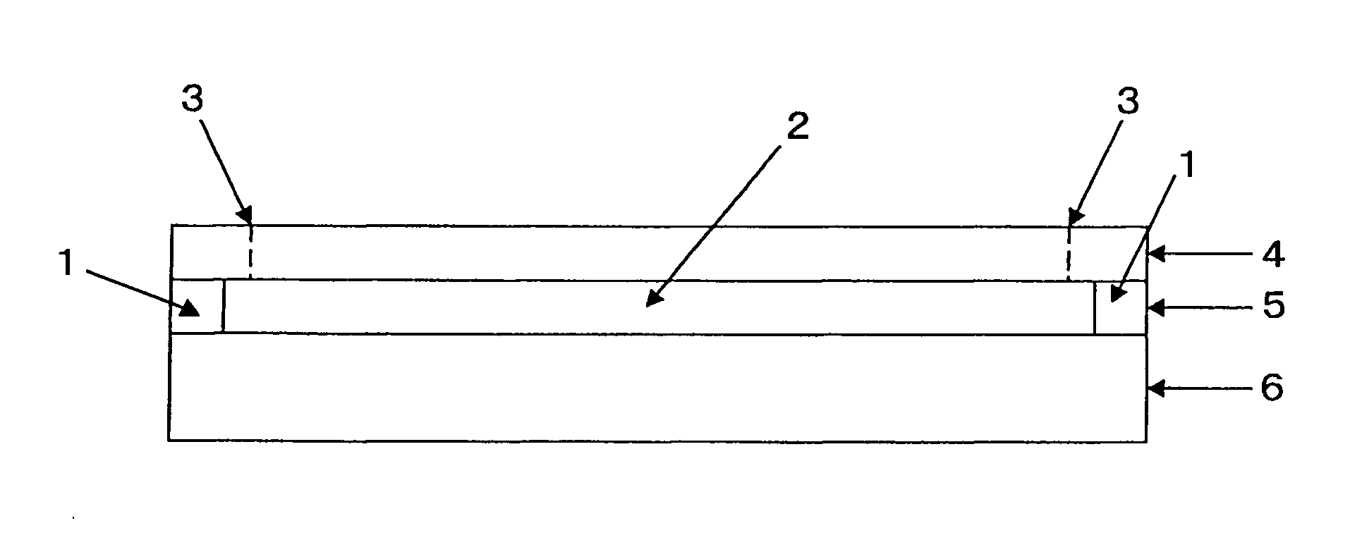
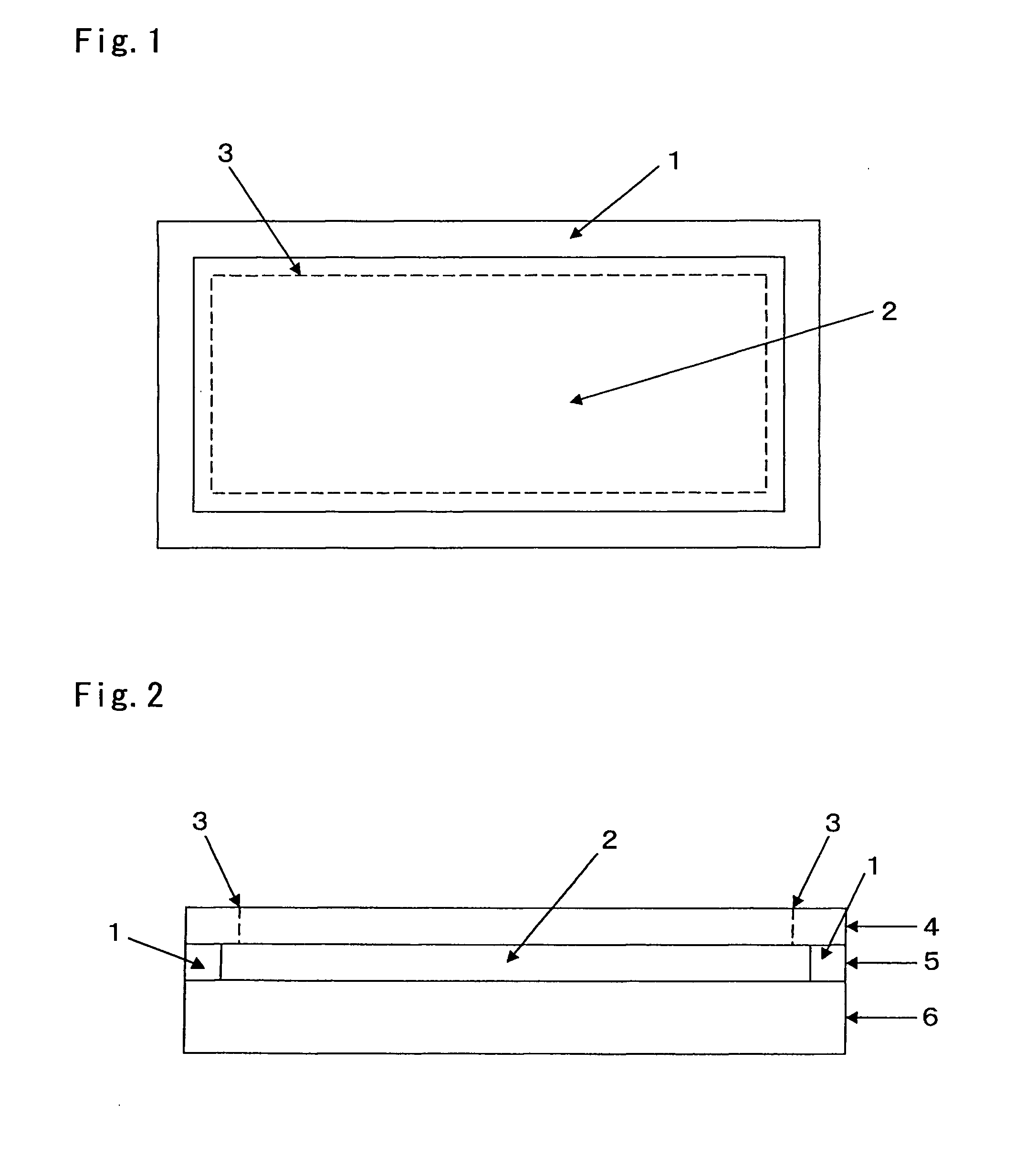
[0056]A silicone rubber monomer (Shin-etsu Chemical Industry's X-34-632T-A and B mixture) was applied onto a supporting substrate of glass (30 cm×50 cm, thickness 1 cm), and then gradually heated from room temperature up to 150° C. and heated in an electric oven for an hour, thereby polymerizing the silicone rubber. The thickness of the adhesive material layer thus formed on the supporting substrate was 300 μm, and the adhesive strength thereof was 6 newtons (N).

(B) Adhesive Strength Controlling Step:

[0057]Next, a metal mask was put on the adhesive material layer, and introduced into a dry-etching device, in which this was subjected to oxygen plasma treatment. The opening of the metal mask used herein was 24 cm×40 cm, and the mask was so set that its opening could be in the center of the supporting substrate of glass. The oxygen plasma treatment condition was as follows: The oxygen flow rate was 50 sccm, the pressure was 0.5 Torr, the power...

Example

EXAMPLE 2

[0065]In (A) of Example 1, a double-face adhesive tape of silicone-based adhesive (Teraoka Seisakusho's 760H#25) was applied to the supporting substrate of glass, in place of using the silicone rubber monomer. In this step, the double-face adhesive, from which the protective film on one surface had been removed, was stuck to the supporting substrate of glass. For bonding the two, the same vacuum thermal bonding device as in Example 1(C) was used under the same condition as therein. After thus bonded, this was taken out of the device, and the protective film on the other surface was removed. The adhesive strength of the supporting substrate was 8.8 newtons. Next, a metal mask was put on the adhesive material layer under the same condition as in Example 1(B), and put into a dry etching device, in which this was subjected to oxygen plasma treatment. The adhesive strength of the peripheral region on which the mask was put and the adhesive strength of the center part that had be...

Example

COMPARATIVE EXAMPLE 1

[0067]An amorphous silicon TFT was fabricated in the same manner as in Example 1, for which, however, the adhesive material controlling step (B) was omitted (device 3). The adhesive strength of the adhesive material before bonding to the plastic substrate was the same both in the peripheral part and in the center part thereof, and was 6 newtons. However, in the final step of peeling the plastic substrate, it could not be peeled off with ease since its adhesive strength was too high. When the peeling force was increased so as to peel the substrate, then the TFT peeled away from the plastic substrate, and, after all, the electric properties of the TFT could not be determined.


PUM

PropertyMeasurementUnit
Forceaaaaaaaaaa
Forceaaaaaaaaaa
Pressureaaaaaaaaaa

Abstract

A method for fixing a plastic substrate, comprising (1) applying or sticking an adhesive material onto a supporting substrate to form an adhesive material layer on the supporting substrate, (2) applying selective adhesive strength controlling treatment to the adhesive material layer to form at least two regions of a low adhesive strength region and a high adhesive strength region, and (3) applying under pressure a plastic substrate to the adhesive material layer at most 300 Torr.

Description

BACKGROUND OF THE INVENTION[0001]1. Field of the Invention[0002]The present invention relates to a plastic substrate and to a method for producing a circuit substrate. Concretely, the invention relates to a method for producing a thin-film laminate device comprising a plastic substrate, and a liquid-crystal display device, in particular to a method for producing various thin-film laminate devices such as flat panel displays (FPD), for example, a liquid-crystal display device with a circuit pattern formed on a plastic film, an organic EL display device, a plasma display panel (PDP), an electrochromic display device, an electroluminescent display device, a field emission display device (FED), etc.; as well as various sensors such as two-dimensional image detectors, and print wiring boards.[0003]2. Description of the Related Art[0004]Heretofore, it has been investigated to thin a substrate for the purpose of reducing the weight of flat panel displays such as typically liquid-crystal di...

Claims


Application Information

Patent Timeline
IPC IPC(8): B32B37/02
CPCB32B37/0076B32B37/12H05K1/0393H05K3/007H05K3/386Y10T156/1052H05K2203/0156H01L21/6835H01L2221/68318H01L2221/6835H01L2221/68381H05K2203/0152
Inventor TADAKUMA, YOSHIO
Owner FUJIFILM CORP
Why Eureka
Try Eureka