Silicide strapping in imager transfer gate device

a transfer gate and shielding technology, applied in semiconductor devices, diodes, radiation controlled devices, etc., can solve problems such as image lag, bright point defect leakage problem, and inability to use pixels, and achieve low lag performance and high barrier

Active Publication Date: 2008-06-05
OMNIVISION TECH INC +1
View PDF6 Cites 45 Cited by
  • Summary
  • Abstract
  • Description
  • Claims
  • Application Information

AI Technical Summary

Benefits of technology

[0014]Preferably, the CMOS imager of the invention including a transfer gate device having two workfunctions (n-type and p-type gate poly) and a silicide strap cooperatively exhibit a high barrier at the photodiode for dark current while a low barrier is provided at the floating diffusion for low lag performance. The silicide strap prevents the diodic behavior from allowing one or the other side of the gate to float to an indeterminate voltage.

Problems solved by technology

However, the pinned photodiode configuration may cause image lag due to the incomplete transfer of charge from the photodiode to the floating node.
Additionally, in the design of the CMOS APS cell 10′ it has been noticed that the presence of silicide contact regions (not shown) formed over the floating node diffusions, in the array, causes a bright point defect leakage problem.
That is, due to the additional presence of formed silicide contacts over these diffusions, it has been found that occasional pixels see silicide “spikes” which leak current at levels high enough to make that pixel unusable.
Unfortunately, however, with the absence of the silicide from imagers with a transfer gate with n and p regions, each CMOS APS cell gate polysilicon formed with the built-in diode within the gate prevents the entire gate from being contacted.
That is, a contact which only connects either the n-type or p-type side of the polysilicon gate will not be adequately connected to the other polarity of the gate poly layer.
This results in a time dependent voltage on the uncontacted portion of the gate.

Method used


Image

  • Silicide strapping in imager transfer gate device
  • Silicide strapping in imager transfer gate device
  • Silicide strapping in imager transfer gate device

Examples


Embodiment Construction

[0041]Prior to describing the present invention in detail, it is instructive to note that the present invention is preferably used in, but not limited to, a CMOS active pixel sensor. Active pixel sensor (APS) refers to an active electrical element within the pixel, other than transistors functioning as switches. For example, the floating diffusion or amplifier are active elements. CMOS refers to complementary metal oxide silicon type electrical components such as transistors which are associated with the pixel, but typically not in the pixel, and which are formed when the source / drain of a transistor is of one dopant type and its mated transistor is of the opposite dopant type. CMOS devices include some advantages one of which is it consumes less power.

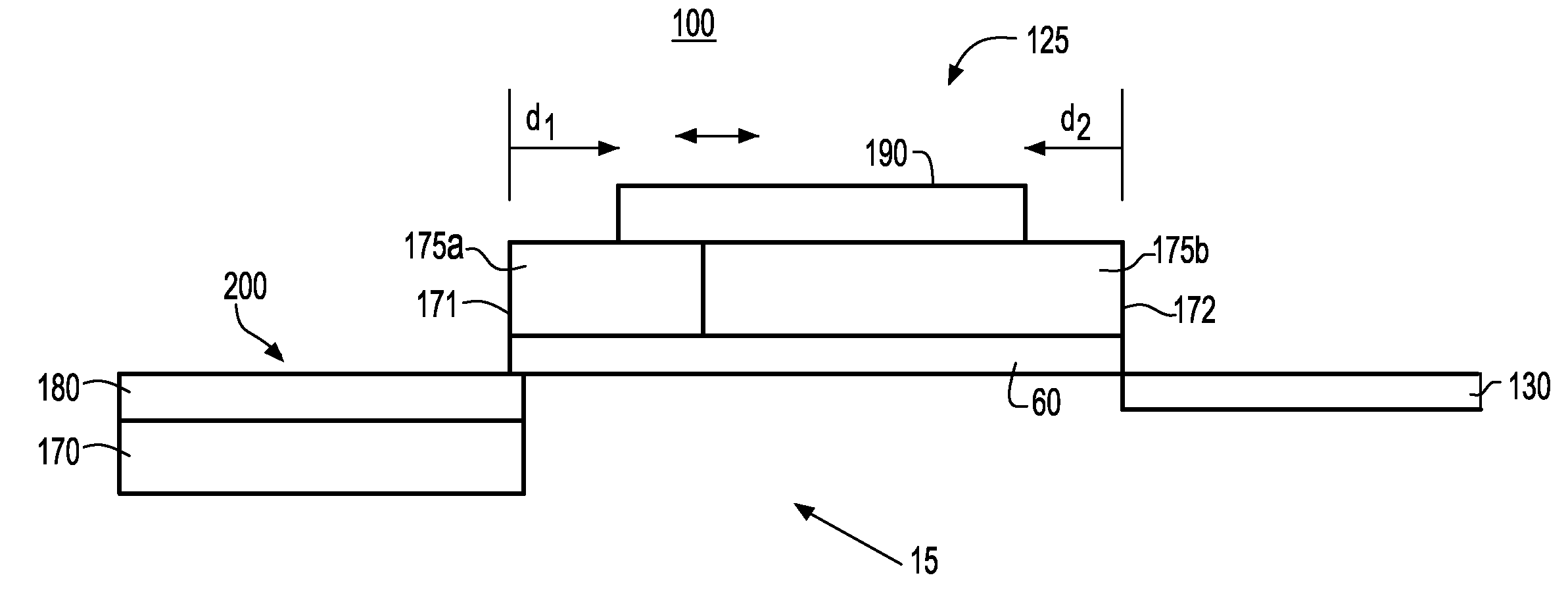
[0042]FIG. 4 illustrates, through a cross-sectional view, a back end of line CMOS imager APS 100 including photosensing device, e.g., photodiode 200, and silicon-containing, e.g., polysilicon, transfer gate 125 according to a first em...


PUM


Abstract

A CMOS active pixel sensor (APS) cell structure having dual workfunction transfer gate device and method of fabrication. The transfer gate device comprises a dielectric layer formed on a substrate and a dual workfunction gate conductor layer formed on the dielectric layer comprising a first conductivity type doped region and an abutting second conductivity type doped region. The transfer gate device defines a channel region where charge accumulated by a photosensing device is transferred to a diffusion region. A silicide structure is formed atop the dual workfunction gate conductor layer for electrically coupling the first and second conductivity type doped regions. In one embodiment, the silicide contact is smaller in area dimension than an area dimension of said dual workfunction gate conductor layer. Presence of the silicide strap prevents the diodic behavior from allowing one or the other side of the gate to float to an indeterminate voltage.

Description

FIELD OF THE INVENTION [0001]The present invention relates to semiconductor optical image sensors, and particularly, to a novel CMOS (complementary metal oxide semiconductor) image sensor cell structure exhibiting reduced lag, higher capacity and lower dark current.DESCRIPTION OF THE PRIOR ART [0002]CMOS image sensors are beginning to replace conventional CCD sensors for applications requiring image pick-up such as digital cameras, mobile telephones, cellular telephones, pervasive digital devices such as PDA's (personal digital assistant), personal computers, medical devices, and the like. Advantageously, CMOS image sensors are fabricated by applying present CMOS fabricating process for semiconductor devices such as photodiodes or the like, at low costs. Furthermore, CMOS image sensors can be operated by a single power supply so that the power consumption for that can be restrained lower than that of CCD sensors, and further, CMOS logic circuits and like logic processing devices are...

Claims


Application Information

Patent Timeline
Patent Type & Authority Applications(United States)
IPC IPC(8): H01L27/146H01L31/18
CPCH01L27/14609H01L27/14689H01L27/14643H01L27/146
Inventor ADKISSON, JAMES W.ELLIS-MONAGHAN, JOHN J.GUIDASH, R. MICHAELJAFFE, MARK D.NELSON, EDWARD T.RASSEL, RICHARD J.STANCAMPIANO, CHARLES V.
Owner OMNIVISION TECH INC
Why Eureka
Try Eureka