Semiconductor Device And Method For Manufacturing Same

a technology of semiconductor devices and semiconductors, applied in the direction of semiconductor devices, basic electric elements, electrical appliances, etc., can solve the problems of comparatively high forward voltage uf, large sturdiness, reverse current, etc., and achieve the effect of high field strength and great sturdiness

Inactive Publication Date: 2008-06-05
ROBERT BOSCH GMBH
View PDF12 Cites 30 Cited by
  • Summary
  • Abstract
  • Description
  • Claims
  • Application Information

AI Technical Summary

Benefits of technology

[0005]Example embodiments of the present invention provide that injection of so-called “hot” charge carriers is prevented. This is achieved in that the high field strength occurring in a breakdown is not near the sensitive oxide layer because the breakdown voltage of the integrated PN diode is lower than the breakdown voltages of the Schottky diode and the MOS structure. The semiconductor device is therefore characterized by a particularly great sturdiness, which permits reliable use of the semiconductor device in the electrical system of a motor vehicle, in particular in the...

Problems solved by technology

Advantages of PN diodes include low reverse current and great sturdiness.
However, the main disadvantage is a comparatively high forward voltage UF.
At room temperature, current begins to flow only at a forward voltage UF of approximately 0.7 V. Under normal operating conditions at which the current density is approximately 500 A/cm2, forward voltage UF increases to more than 1 V. This results in a decline in efficiency.
Schottky diodes have not yet been used in the generator system of a motor vehicle.
This may be attributed to some significant disadvantages of a Schottky diode which make such an application appe...

Method used


Image

  • Semiconductor Device And Method For Manufacturing Same
  • Semiconductor Device And Method For Manufacturing Same
  • Semiconductor Device And Method For Manufacturing Same

Examples


example embodiment

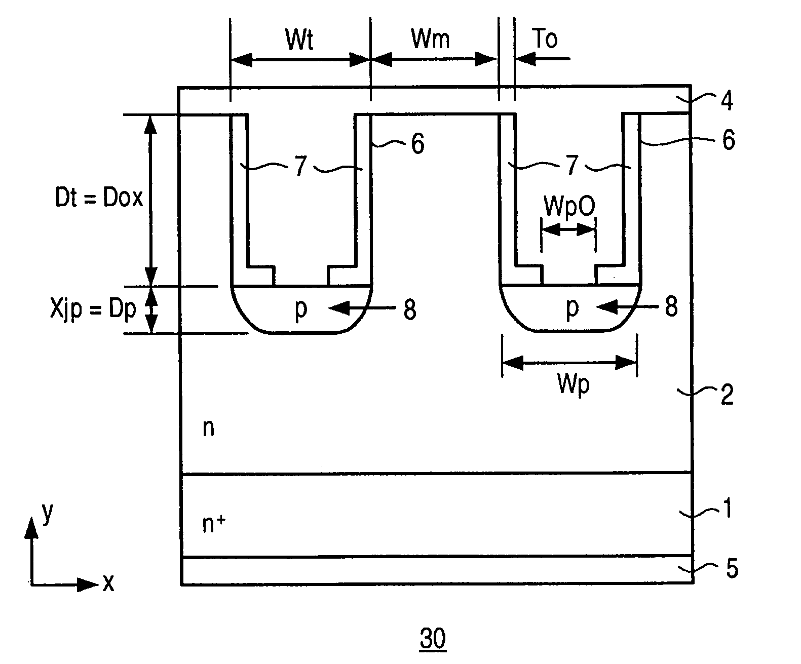
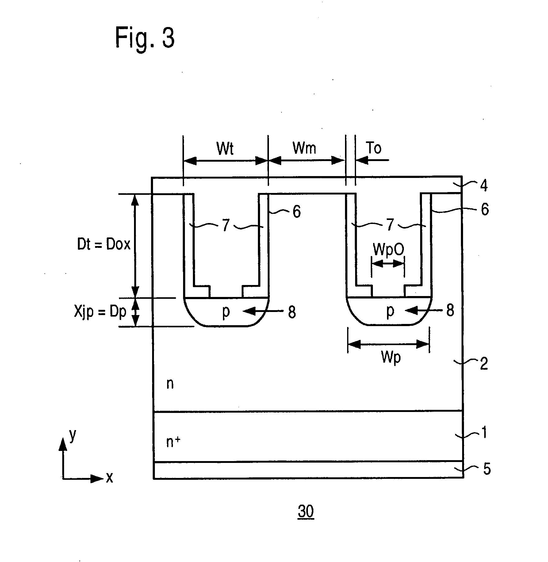
[0021]A method for manufacturing semiconductor device 30 is described below (example embodiment according to FIG. 3), reference also being made to the flow chart in FIG. 5. This also starts with an n+ substrate 1 (step 50) to which an n-layer 2 is applied, e.g., by epitaxy (step 51). Trenches 6 are created in n-layer 2 by an etching process (step 52). Next the bottoms and side walls of trenches 6 are covered with an oxide layer (step 53). In a subsequent etching step (step 54), the oxide layer covering the bottoms of trenches 6 is partially removed. This creates a mask of width Wp0 for the subsequent diffusion process. For this, the region of trenches 6 from which the oxide layer has been removed is first covered with a p dopant, e.g., boron (step 55). This may be done by deposition from the gas phase or by ion implantation. Next the diffusion process is performed (step 56) in which boron diffuses into n-layer 2 and forms p regions 8. Finally, contact layers 4 and 5 are again applie...


PUM


Abstract

A semiconductor device (20) comprising a trench MOS barrier Schottky diode having an integrated PN diode and a method for manufacturing same are described.

Description

FIELD OF THE INVENTION[0001]The present invention relates to a semiconductor device and a method for manufacturing same.BACKGROUND INFORMATION[0002]In modern motor vehicles, more and more functions are being implemented using electrical components. This results in an ever-increasing demand for electric power. To meet this demand, the efficiency of the generator system in the motor vehicle must be increased. So far, PN diodes have been usually used as Zener diodes in the generator system of the motor vehicle. Advantages of PN diodes include low reverse current and great sturdiness. However, the main disadvantage is a comparatively high forward voltage UF. At room temperature, current begins to flow only at a forward voltage UF of approximately 0.7 V. Under normal operating conditions at which the current density is approximately 500 A / cm2, forward voltage UF increases to more than 1 V. This results in a decline in efficiency.[0003]On the basis of theoretical considerations, the Schot...

Claims


Application Information

Patent Timeline
IPC IPC(8): H01L29/872H01L21/329
CPCH01L29/66143H01L29/8725H01L29/872H01L29/861
Inventor GOERLACH, ALFREDQU, NING
Owner ROBERT BOSCH GMBH
Why Eureka
Try Eureka