Electric current collector, electrode and charge accumulating device
a technology current collector, which is applied in the field of electric current collector, can solve the problems of increased internal resistance, reduced serious environmental pollution, and achieve the effect of suppressing enhancing internal resistance, and reducing the output characteristics of charge accumulating devi
- Summary
- Abstract
- Description
- Claims
- Application Information
AI Technical Summary
Benefits of technology
Problems solved by technology
Method used
Image
Examples
example 1
[0066]First, an aluminum foil (manufactured by NIPPON FOIL MFG. CO., LTD., 1N30 Material pursuant to the provisions in JIS) comprising a H material, a cold rolled material which is not annealed, having a thickness of 15 μn was prepared. This aluminum foil has not been subjected to a heat treatment.
[0067]This aluminum foil was fixed on the surface of a porous ceramic material. From the back surface side of the ceramic material, an aluminum foil was intimately attached onto the ceramic by evacuation.
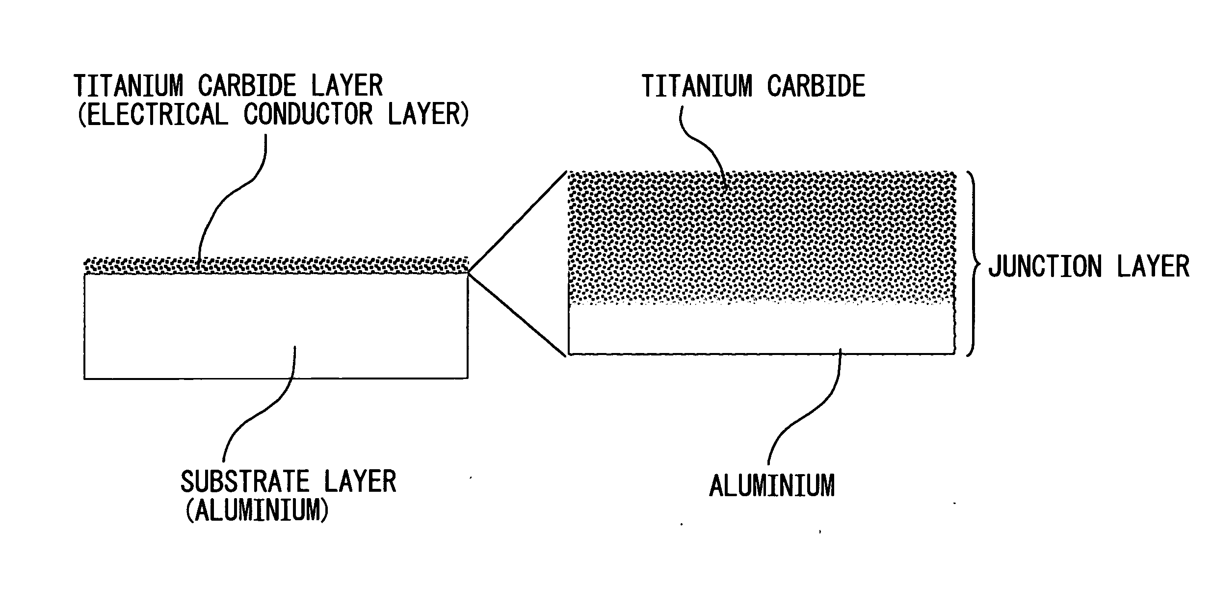
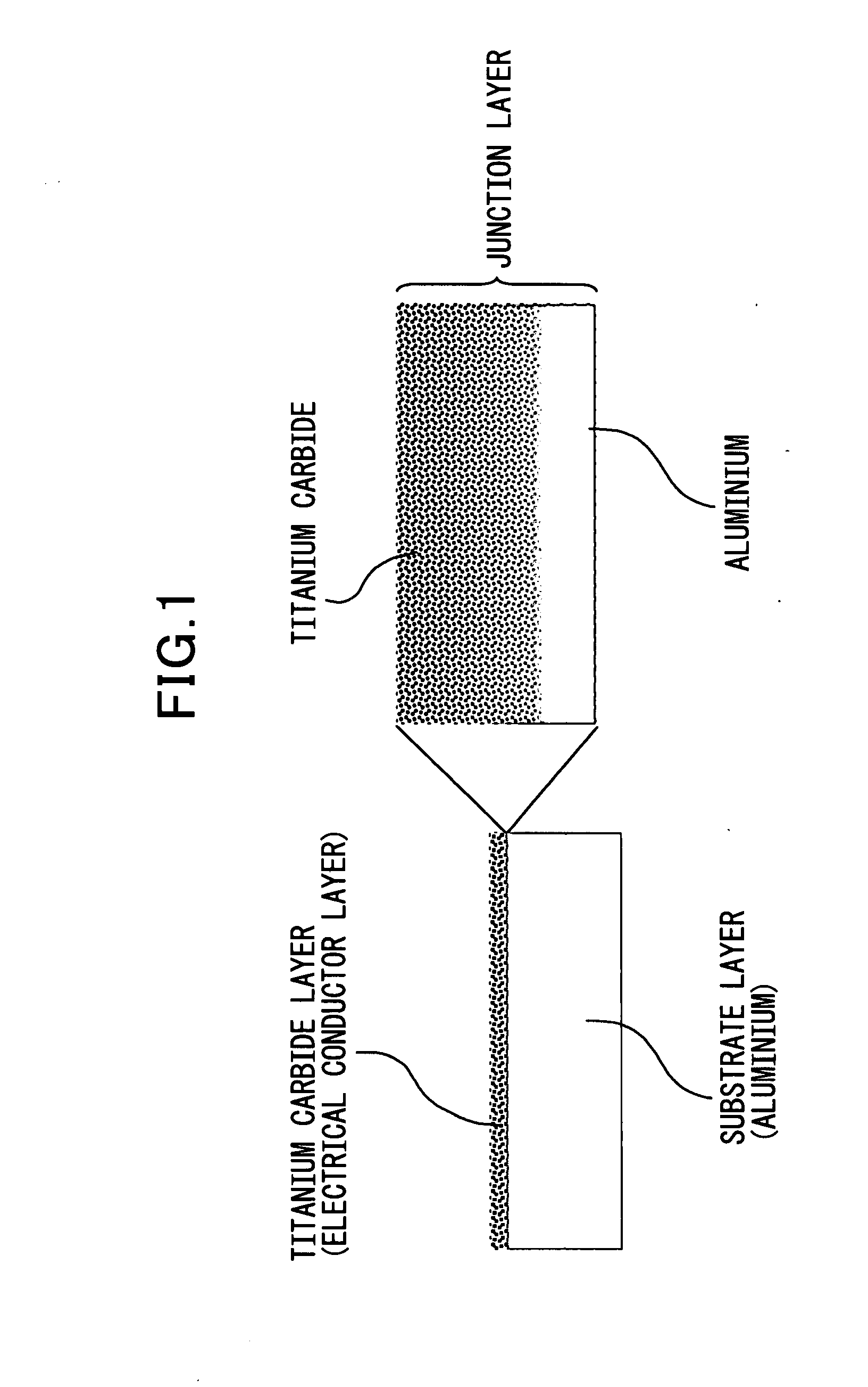
[0068]Titanium carbide particles (manufactured by SHINNIHONKINZOKUKOGYO CO., LTD.) with a mean particle size of 1.5 μm were sprayed under ordinary temperature onto the surface of the aluminum foil intimately attached on the surface of the ceramic material. The spraying of the titanium carbide particles was performed by scanning the nozzle, until a titanium carbide coating (titanium carbide layer) was formed on an area of a 50 mm square on the surface of the aluminum foil. The maximum flow ...
example 2
[0072]An electric current collector of this Example was manufactured in a manner similar to Example 1 except that particles sprayed onto the surface of the aluminum foil were graphite particles having a mean particle size of 2 μm.
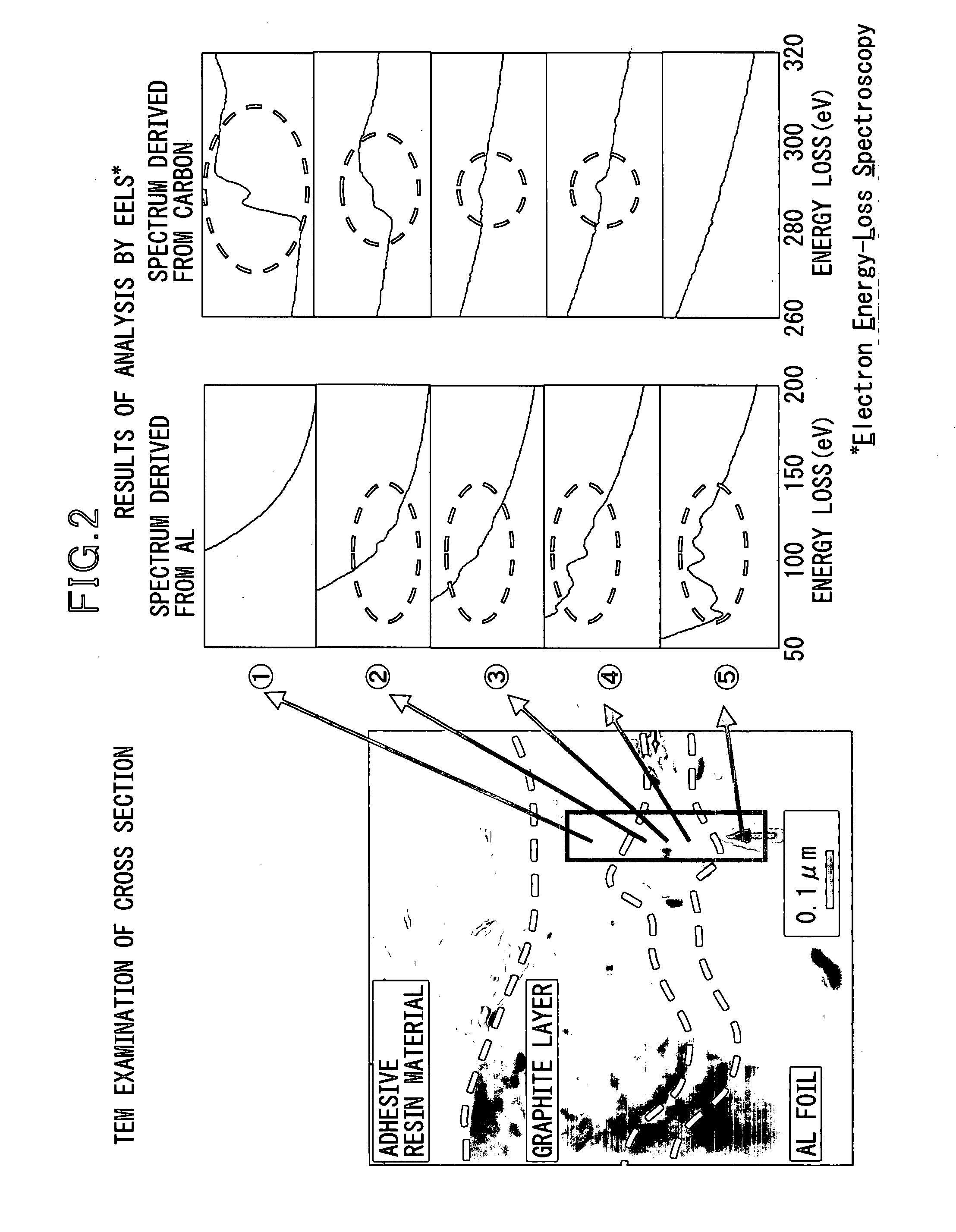
[0073]When the cross section of the electric current collector of this Example was examined with a transmission electron microscope (TEM), it was confirmed that a graphite layer (an electrical conductor layer) was formed at a thickness of 0.3 to 0.5 μm from the surface, and a junction layer in which graphite was diffused (mixed) in aluminum was formed at a thickness of 0.15 to 0.3 μm in the inside of a graphite layer, and the rest was formed with a substrate layer composed of aluminum.
[0074]It was confirmed by the electron energy-loss spectroscopy (EELS) that the ratio of graphite contained therein gradually increases from the substrate layer side to the graphite layer in the junction layer (FIG. 2). Also, no passivation coating was confirmed in the interfa...
example 3
[0098]First, an electric current collector was manufactured in a method similar to that in Example 1.
[0099]Subsequently, 87 parts by weight of LiNiO2 as the positive-electrode active material, 10 parts by weight of graphite, 1 part by weight of CMC and 1 part by weight of polyethylene oxide (PEO) as the electrically conductive auxiliary material, and 1 part by weight of PTFE as the binder were prepared, and were dispersed in water to prepare a positive-electrode combined paste.
[0100]The positive-electrode combined paste thus prepared was applied on both surfaces of an electric current collector, kept at 80° C. for 30 minutes, and then dried. It was pressed with a hand press machine at a pressure of 12 kN. By pressing, the density of the electrode combined material on the surface of the electric current collector plate became 2 g / cm3.
[0101]In this way, a positive electrode for the lithium battery of this Example was manufactured.
PUM
| Property | Measurement | Unit |
|---|---|---|
| thickness | aaaaa | aaaaa |
| thickness | aaaaa | aaaaa |
| median diameter | aaaaa | aaaaa |
Abstract
Description
Claims
Application Information


