

Conjugated Organic Molecules for Molecular Electronic Devices
a technology of molecular electronic devices and conjugated organic molecules, applied in the field of molecules, can solve the problems of difficult to distinguish semiconducting tubes from metallic and insulating tubes, and the assembly of transistors in this way may or may not work, and achieve the effects of not and easy processing of carbon nanotubes
- Summary
- Abstract
- Description
- Claims
- Application Information
AI Technical Summary
Benefits of technology
Problems solved by technology
Method used
Image

Examples
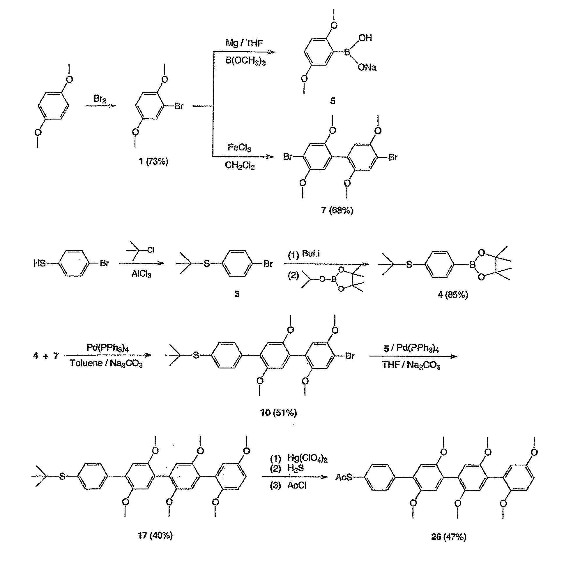
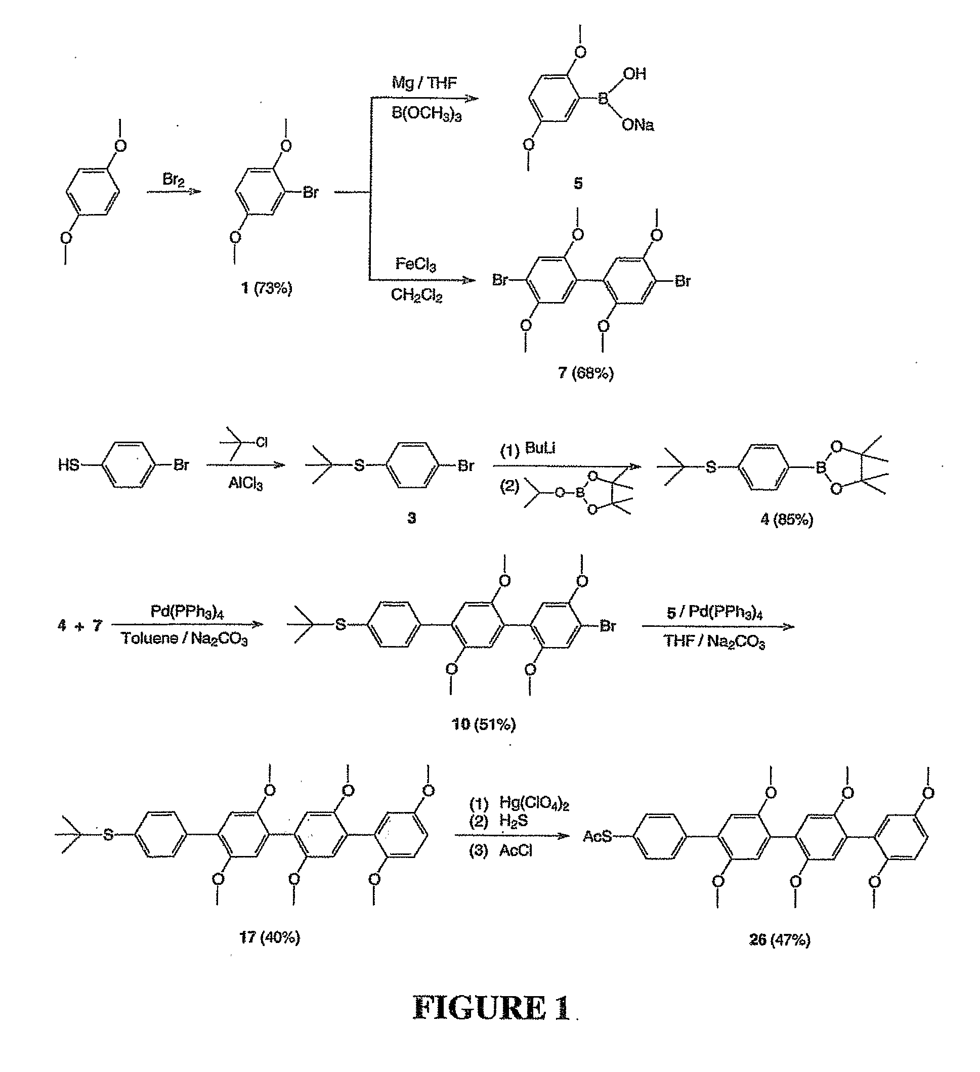
example 1
Preparation of 2,5-dimethoxybromobenzene (1)
[0099]In a one liter round-bottom flask, a solution of bromine (16.0 g, 100 mmol) in acetic acid (50 ml) was added dropwise to a solution of 1,4-dimethoxybenzene (13.8 g, 100 mmol) in chloroform and methanol (400 ml) at 0° C. After stirring for 3 hours, 500 ml of saturated Na2CO3 solution was added. The organic layer was washed with water, brine and dried over sodium sulfate. After the solvent was removed on a rotary evaporator, the residue was distilled under reduced pressure to yield 15.8 g of 2,5-dimethoxybromobenzene (yield 73%) 1HNMR (CDCl3) δ7.148 (s, 1H), 6.859 (s, 2H), 3.869 (s, 3H), 3.785 (s, 3H).
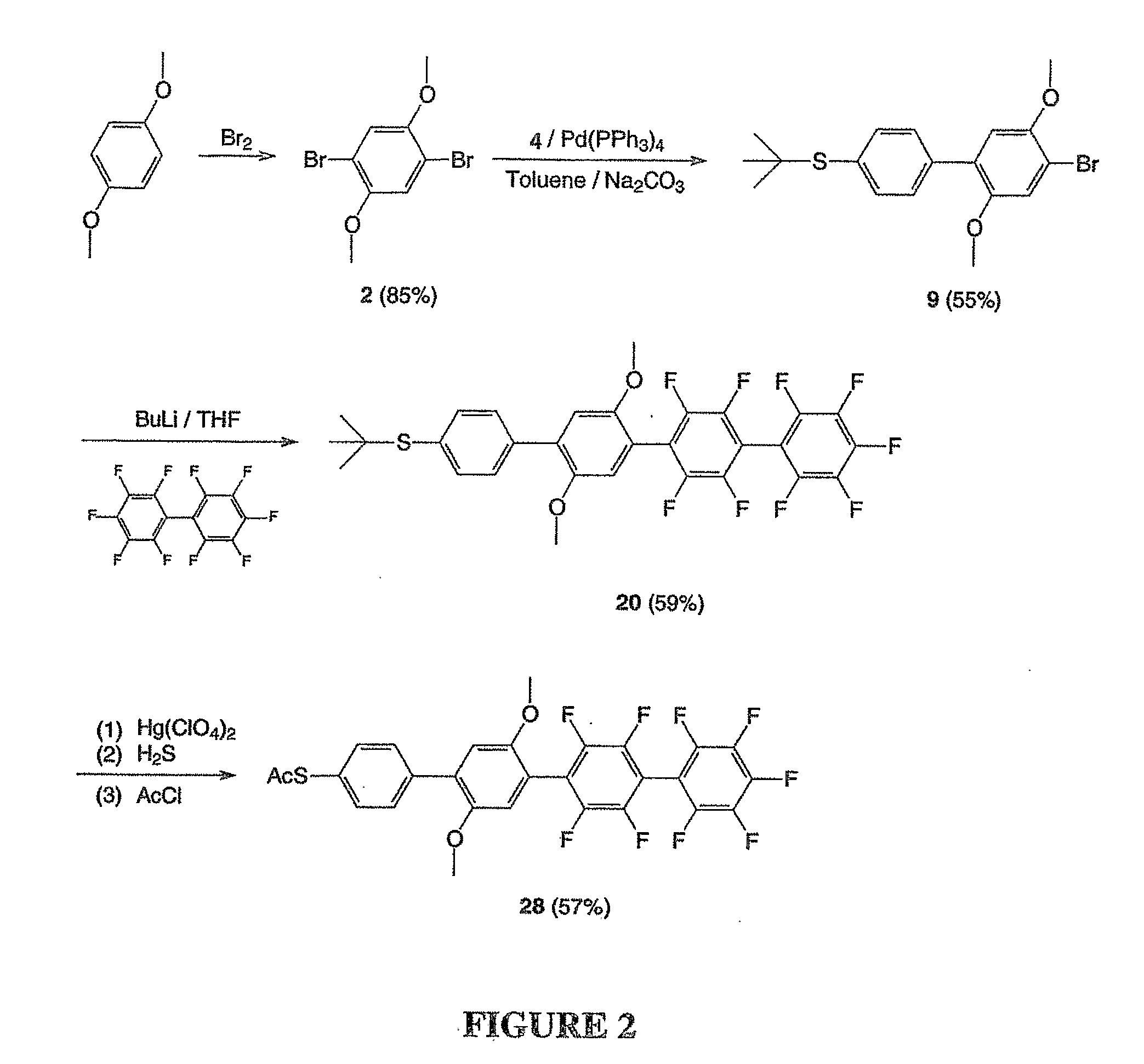
example 2
Preparation of 2,5-dibromo-1,4-dimethoxybenzene (2)
[0100]In a one liter round-bottom flask, a solution of bromine (35.2 g, 220 mmol) in chloroform (50 ml) was added dropwise to a solution of 1,4-dimethoxybenzene (13.8 g, 100 mmol) in chloroform (400 ml) under 0° C. After stirring for 3 hours, 100 ml of saturated Na2CO3 solution was added. The organic layer was washed with water, brine, and dried over sodium sulfate. The solvent was removed on a rotary evaporator and the residue was performed recrystallization from ethanol to afford pure 2,5-dibromo-1,4-dimethoxybenzene (25.8 g, 85%). 1HNMR (CDCl3) δ7.128 (s, 2H), 3.873 (s, 6 H).
example 3
Preparation of 4-tert-butylthio-bromobenzene (3)
[0101]In a 50 ml round-bottom flask, a mixture of 20 ml of tert-butyl chloride and 9.5 g of 4-bromothiophenol was stirred until all the solids dissolved, then a catalytic amount of AlCl3 was added. After stirring for 2 hours, the mixture was poured into 100 ml of ice water and extracted with hexane twice. The solvent was removed and the crude product was purified with flash column (used hexane as the eluent) to offer 10.5 g of 4-tert-butylthio-bromobenzene. The obtained product was used in synthesis reactions without further purification.
PUM
| Property | Measurement | Unit |
|---|---|---|
| Angle | aaaaa | aaaaa |
| Electrical conductor | aaaaa | aaaaa |
Abstract
Description
Claims
Application Information