Chip scale package structure and method for fabricating the same

Active Publication Date: 2008-06-12
SILICONWARE PRECISION IND CO LTD
View PDF9 Cites 26 Cited by
  • Summary
  • Abstract
  • Description
  • Claims
  • Application Information

AI Technical Summary

Benefits of technology

[0019]In addition, according to the present invention, the encapsulant can further be ground to expose the inactive surface of the chip, thereby enhancing the heat dissipation efficiency; furthermore, it can apply at least a dielectric layer and a plurality of second conductive traces between the first conductive traces and the solder mask, thus enhances the flexibility of the first conductive traces layout of the package structure.
[0020]Therefore, the chip scale package structure and a method for fabricating the same according to the present invention mainly first form a plurality of well-aligned metal pads on the predetermined positions of the carrier, thus the relative position of each metal pad can be accurately located, next, mount a plurality of chips on the carrier, wherein each chip has a plurality of conductive bumps, and by soldering the conductive bumps to the corresponding metal pads of the carrier, each of the chips is accurately aligned on the carrier, thereby giving the benefit to the subsequent fabrication process, and accordingly avoiding the problems of high production cost, complicated fabrication process, and the practical incapability of effective mass production, etc, according to the fabrication method of the chip scale package structure of the prior art, wherein, it uses the batch-type method to attach a plurality of chips, which have conductive bumps, on an adhesion tape in an array layout, accordingly it can not accurately control the relative attach position for each chip due to the machine inaccuracy

Problems solved by technology

However, the disadvantage of the aforementioned CSP structure is that the application of the redistribution technology or the distribution of the conductive traces on the chip is always restricted by the size of the chip or its active surface area, especially in the situation that the chip integration level is getting higher and the chip size is getting smaller, the chip can not even provide enough or more surface for installing higher number of solder balls for effectively electrically connecting to external devices.
However, the package structure of the aforementioned disclosure has its drawback, when open the plurality of via holes that go through the first dielectric layer to expose the bond pads of the chip by means of laser drilling technology, the plurality of bond pads of the chip are covered by the first dielectric layer, generally it is difficult to aim the laser beam accurately at the solder pad position, consequently the via holes opened can not be aligned accurately to the corresponding bond pad position; since the bond pads of the chip can not completely exposed, it is difficult to ensure the electricity connection quality between the circuit layer and the bond pads, thereby hurting the yield and reliability of the finished products.
Meanwhile, the applying of the first dielectric layer on the tops of the chip and the encapsulant as well as the application of the laser drilling technology increase the production cost and fabrication complexity, and the first dielectric layer has different coefficient of thermal expansion (CTE) from the chip and the encapsulant, in a high temperature environment or a heat circulation situation, the first dielectric layer will produce different thermal

Method used


Image

  • Chip scale package structure and method for fabricating the same
  • Chip scale package structure and method for fabricating the same
  • Chip scale package structure and method for fabricating the same

Examples


second embodiment

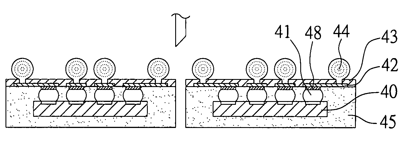
[0044]Please refer to FIG. 6, which is a cross sectional view of a chip scale package structure according to the present invention. As shown in FIG. 6, the chip scale package structure is similar to the one disclosed in the aforementioned embodiment, and the difference is that the part of the encapsulant 45 that covers the inactive surface 402 of the chip 40 can be ground and removed, and thus the inactive surface 402 of the chip 40 is exposed, this helping the heat produced by the operation of the chip 40 to dissipate into the environment, thereby enhancing the heat dissipation efficiency of the package structure.

third embodiment

[0045]Please refer to FIG. 7, which is a cross sectional view of a chip scale package structure according to the present invention. As shown in FIG. 7, the chip scale package structure is similar to the ones disclosed in the aforementioned embodiments, the difference is that after the first conductive traces 42 are formed on the encapsulant 45, first applying at least a dielectric layer 49 on the top of the first conductive traces 42, and then forming a plurality of through holes that go through the dielectric layer 49, thus exposing the predetermined parts of the first conductive traces 42 through the through holes. Next, forming a plurality of second conductive traces 422 on the dielectric layer 49, and having each of the second conductive traces 422 be electrically connected to at least one exposed part of the first conductive traces 42.

[0046]After that, a solder mask 43 is applied on the second conductive traces 422, and then a plurality of openings are formed on the solder mask...


PUM


Abstract

A chip scale package structure and a method for fabricating the same are disclosed. The method includes forming metal pads on a predetermined part of a carrier; mounting chips on the carrier, each of the chips having a plurality of conductive bumps soldered to the metal pads; forming an encapsulant on the carrier to encapsulate the chips and the conductive bumps; removing the carrier to expose the metal pads and even the metal pads with a surface of the encapsulant; forming on the encapsulant a plurality of first conductive traces electrically connected to the metal pads; applying a solder mask on the first conductive traces, and forming a plurality of openings on the solder mask to expose a predetermined part of the first conductive traces; forming a plurality of conductive elements on the predetermined part; and cutting the encapsulant to form a plurality of chip scale package structures.

Description

BACKGROUND OF THE INVENTION[0001]1. Field of the Invention[0002]The present invention generally relates to a semiconductor package structures, and more specifically, to a chip scale package structure and a method for fabricating the same.[0003]2. Description of Related Art[0004]Along with the advancement of the semiconductor technology, semiconductor products have been developed in a variety of different package types. In the pursuing of a lighter, thinner and smaller semiconductor package structure, a chip scale package (CSP) structure has been developed. The feature of this chip scale package structure is that its size is equal to or a little bit bigger than the chip size.[0005]U.S. Pat. Nos. 5,892,179, 6,103,552, 6,287,893, 6,350,668, and 6,433,427 disclose a conventional CSP structure, which applies build-up layers directly on the top of the chip without using a chip carrier such as a substrate or a lead frame, and by means of the redistribution layer (RDL) technology to redistr...

Claims


Application Information

Patent Timeline
IPC IPC(8): H01L21/00
CPCH01L21/561H01L2224/0401H01L23/3114H01L24/19H01L24/97H01L2224/04105H01L2224/20H01L2224/97H01L2924/01029H01L2924/01046H01L2924/01079H01L2924/01082H01L2924/15311H01L2924/18161H01L21/568H01L2224/16225H01L2924/01033H01L2224/82H01L24/96H01L2224/12105H01L2924/18162H01L2924/351H01L2924/00
Inventor PU, HAN-PINGHUANG, CHIEN-PINGHSIAO, CHENG-HSU
Owner SILICONWARE PRECISION IND CO LTD
Why Eureka
Try Eureka