This helps you quickly interpret patents by identifying the three key elements:
Problems solved by technology
Method used
Benefits of technology
Benefits of technology
[0012]Accordingly, the present invention has been made to solve the above-described shortcomings occurring in the prior art, and an object of the present invention is to provide a III-nitride compound semiconductor light emitting device with improved performance, in which the barrier layer(s) of a multiple-quantum-well active layer have a sandwich structure of InGaN / GaN / InGaN, not a single-layer structure, so that the disadvantages of the prior multiple-quantum-well layer stacks can be overcome and only their advantages can be taken.Technical Solution
[0017]According to the present invention, a high-efficiency / high-output light emitting device with high-current and high-temperature properties can be obtained, and it is possible to easily achieve a high-efficiency green light emission at a wavelength equal to or over 500 nm, and high-efficiency near UV light emission.
Problems solved by technology
However, the InGaN / GaN multiple-quantum-well active layer has a limitation in that the GaN barrier layers 13a should be grown at low temperature since the growth temperature of the InGaN well layers 13b is about 200-350° C. lower than the general growth temperature of high-quality GaN.
Another disadvantage is that the strain of the InGaN well layers 13b and the GaN barrier layers 13a needs to be optimized only with-the thickness of the InGaN well layers 13b and the GaN barrier layers 13a.
However, the InGaN / InGaN multiple-quantum-well active layer has a disadvantage in that it has low stability in high-current or high-temperature operations as compared to the InGaN / GaN multiple-quantum-well layer.
However, this approach has a disadvantage in that, in epitaxial growth of the nitride compound, the deposition of an aluminum (Al)-containing nitride compound, which is difficult to remove easily, occurs within a reactor.
This results in a great reduction in mass production.
Another disadvantage with the InGaN / InGaN multiple-quantum-well active layer is that the performance and properties of a light emitting diode including the active layer are sensitive to a small change in, the indium composition of the InGaN barrier layer 13a′ thus making the mass production of the diode difficult.
Thus, growing a material with the precursor maintained at a constant composition is relatively difficult compared to other precursors.
Image
Click on the blue label to locate the original text in one second.
Reading with bidirectional positioning of images and text.
Examples
embodiment 1
[0025]FIG. 4 is an energy band diagram illustrating a III-nitride compound semiconductor light emitting device according to the first embodiment of the present invention.
[0026]Referring to FIG. 4, the multiple-quantum-well active layer 113 comprises an alternate stacking of the quantum well layers 113b made of InxGa1-xN(0.05113a formed on the quantum well layers 113b.
[0027]The sandwich barrier layers 113a have a sandwich structure comprising the first outer barrier layer 201 formed of InaGa1-aN(0113b, a middle barrier layer 202 formed of AlyGa1-yN(0≦y201, and the second outer barrier layer 203 formed of InbGa1-bN(0202.
[0028]The lowest layer of the active layer 113, which is in contact with the n-InxAlyGazN layer 12, is the first of the quantum well layers 113b, and the highest layer of the active layer 113, which is in contact with the p-InxAlyGazN layer 14, is the last of the quantum well layers 113b.
[0029]Similarly to the quantum well layers 113b, the outer barrier layers 201 an...
embodiment 2
[0041]FIG. 7 is an energy band diagram illustrating a III-nitride semiconductor light emitting device according to a second embodiment of the present invention.
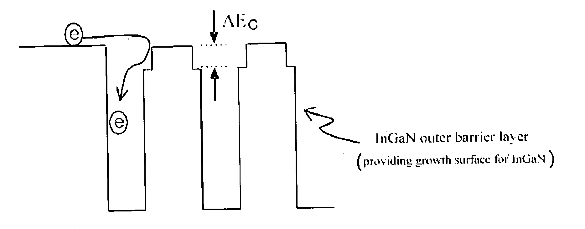
[0042]As shown in FIG. 4, the lowest layer of the active layer 113, which is in contact with the n-InxAlyGazN layer 12, and the highest layer of the active layer 113, which is in contact with the p-InxAlyGazN layer 14, must not be necessarily be the quantum well layers 113b. As shown in FIG. 7, the lowest layer of the active layer 113, which is in contact with the n-InxAlyGazN layer 12, and the highest layer of the active layer 113, which is in contact with the p-InxAlyGazN layer 14, may also be the middle barrier layers 202 of the sandwich barrier layers 113a.
[0043]The structure shown in FIG. 7 is characterized in that all the InGaN quantum well layers can grow on surfaces provided as the InGaN outer barrier layers in the same conditions. Thus, this structure has advantages is that it is more advantageous in achieving an un...
PUM
Abstract
The present invention relates to a III-nitridecompound semiconductorlight emitting device comprising an active layer with the multi-quantum wells interposed between an n-InxAlyGazN(x+y+z=1, 0<x<1, 0<y<1, 0<z≦1) layer and a p-InxAlyGazN(x+y+z=1, 0<x<1, 0<y<1, 0<z<1) layer, wherein the active layer comprises an alternate stacking of a quantum-well layer made of InxGa1-xN(0.05<x<1) and a sandwich barrier layer, the sandwich barrier layer comprising a first outer barrier layer of InaGa1-aN(0<a<0.05), a middle barrier layer of AlyGa1-yN(0<y<1) formed on the first outer barrier layer and a second outer barrier layer of InbGa1-bN(0<b<0.05) formed on the middle barrier layer, thereby a high-efficiency / high-output light emitting device with high-current and high-temperature properties can be obtained, and it is possible to easily achieve a high-efficiency green light emission at a wavelength equal to or over 500 nm, and high-efficiency near UV light emission.
Description
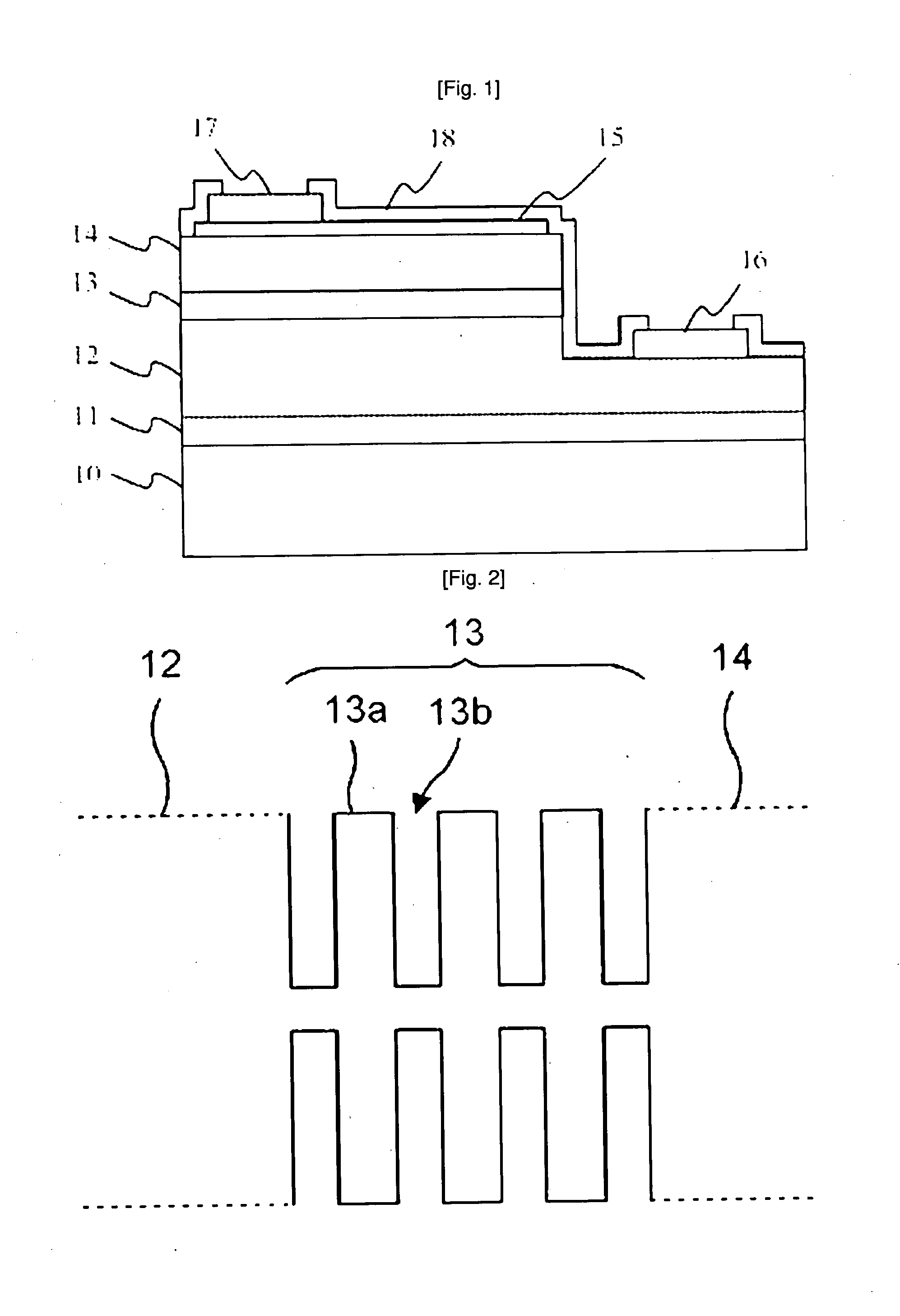
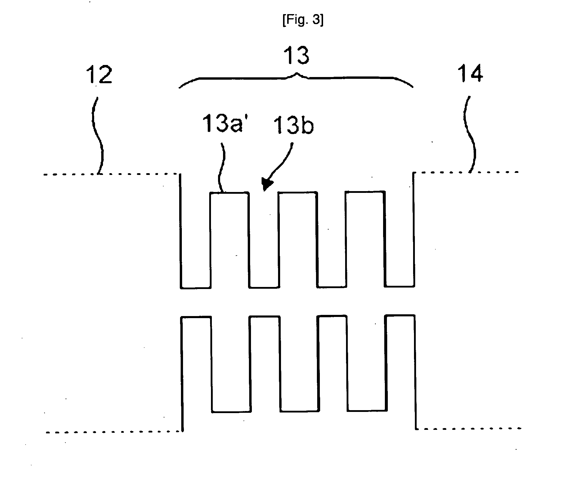
TECHNICAL FIELD [0001]The present invention relates to a III-nitridecompound semiconductorlight emitting device, and more particularly, to a III-nitridecompound semiconductor light emitting device having a multiple-quantum-well (MQW) active layer comprising an alternate stacking of quantum welllayers and sandwich barrier layer(s).BACKGROUND ART [0002]FIGS. 1 to 3 are drawing illustrating a III-nitride compound semiconductor light emitting device according to the prior art. Specifically, FIG. 1 is a cross-sectional view of the III-nitride compound semiconductor light emitting device, FIG. 2 is an energy band diagram showing that the active layer 13 has an InGaN / GaN multiple-quantum-well structure, and FIG. 3 is an energy band diagram showing that the active layer 13 has an InGaN / InGaN multiple-quantum-well structure.[0003]Referring to FIG. 1, to fabricate a nitride compound semiconductor light emitting device according to the prior art, the buffer layer 11, the n-InxAlyGazN layer...
Claims
Application Information
Patent Timeline
Application Date:The date an application was filed.
Publication Date:The date a patent or application was officially published.
First Publication Date:The earliest publication date of a patent with the same application number.
Issue Date:Publication date of the patent grant document.
PCT Entry Date:The Entry date of PCT National Phase.
Estimated Expiry Date:The statutory expiry date of a patent right according to the Patent Law, and it is the longest term of protection that the patent right can achieve without the termination of the patent right due to other reasons(Term extension factor has been taken into account ).
Invalid Date:Actual expiry date is based on effective date or publication date of legal transaction data of invalid patent.

