
High temperature photonic structure for tungstein filament

a technology of photonic structure and tungstein filament, which is applied in the direction of discharge tube/lamp details, gas-filled discharge tubes, nuclear engineering, etc., can solve the problem of reducing the efficiency of the discharge lamp, reducing the energy loss of the lamp to non-visible light output, and not addressing the suppression or conversion of unwanted light emissions. the device, however, suffers from structural instability

Inactive Publication Date: 2008-06-26
GENERAL ELECTRIC CO
View PDF2 Cites 9 Cited by
  • Summary
  • Abstract
  • Description
  • Claims
  • Application Information

AI Technical Summary

Problems solved by technology

Resistively or non-resistively heated light sources, including incandescent and discharge lamps, generally lose a majority of the emitted wavelengths in the infrared region of the spectrum, which translates into what may be as high as a 70% energy loss for the lamp to non-visible light output.
While this technology was able to reduce energy losses with about a 50% efficiency rate, it nonetheless does not address the issue of suppression or conversion of unwanted light emissions.
This device, however, suffers from structural instability at temperatures as low as about 1200° C., even though the melting point of tungsten is far above that.
The foregoing, while advancing the technology to some degree, fail to fully address the issue of wavelength suppression and shift to generate emissions of the shifted wavelengths in the visible range, thus increasing lamp efficiency.

Method used


Image

  • High temperature photonic structure for tungstein filament
  • High temperature photonic structure for tungstein filament
  • High temperature photonic structure for tungstein filament

Examples


Embodiment Construction

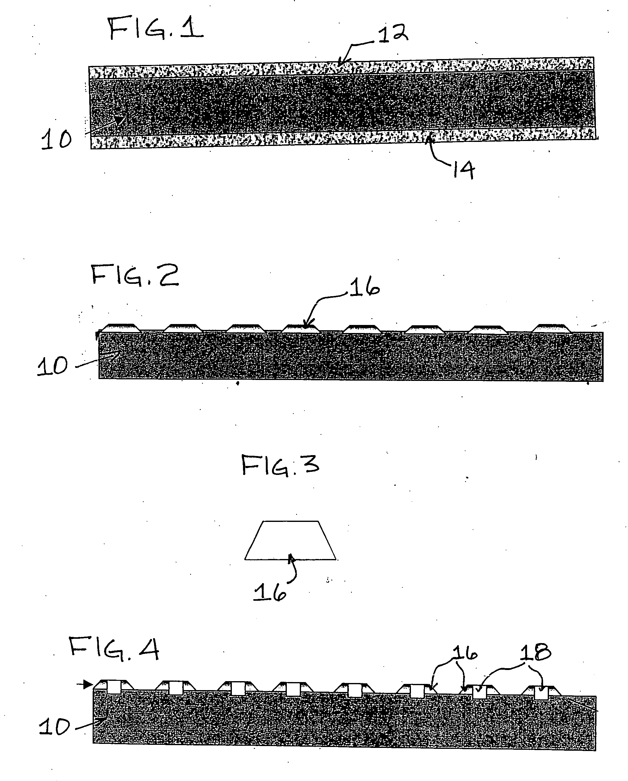
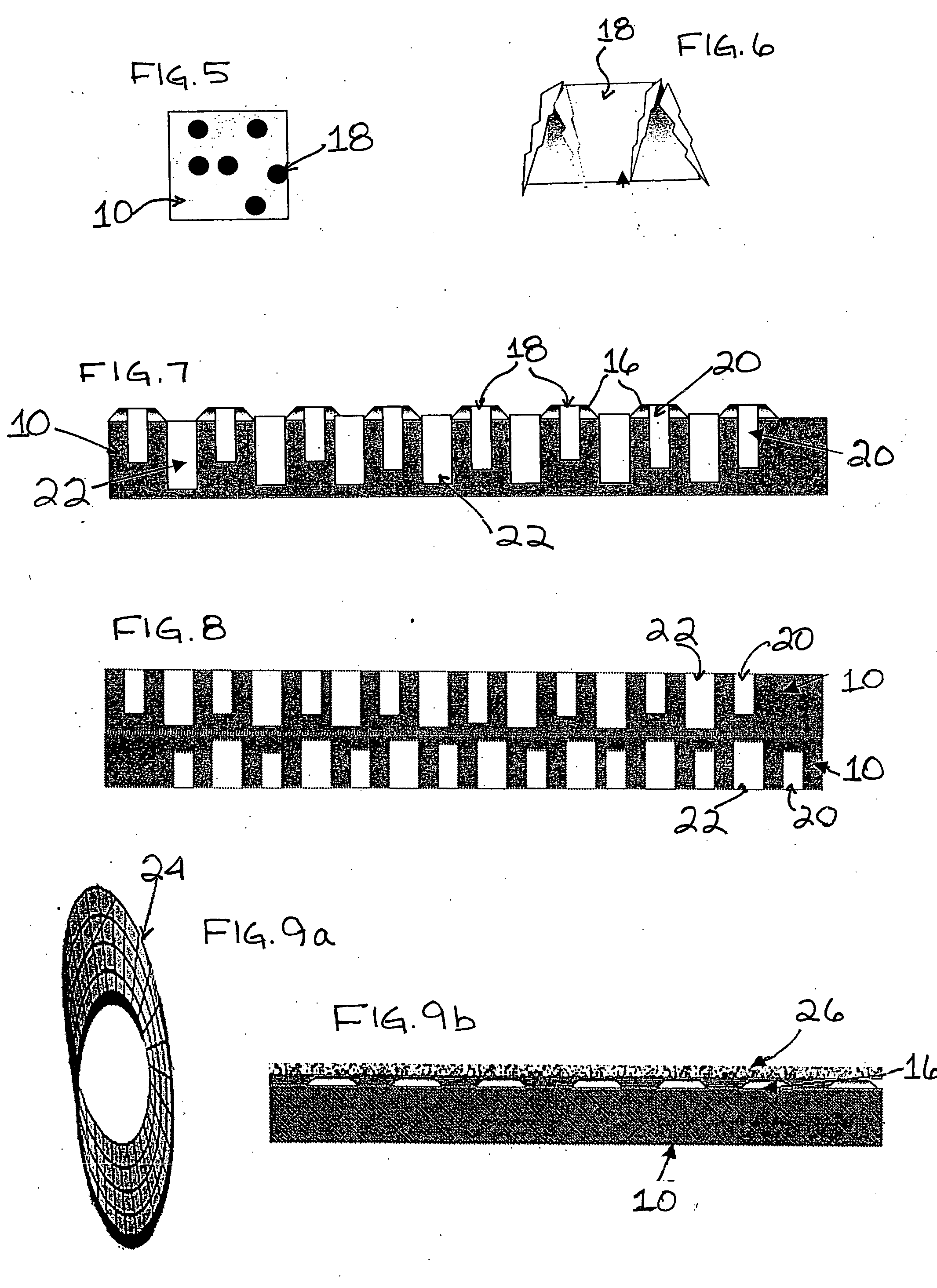
[0020]With reference to FIG. 1, substrate 10, which may be tungsten, magnesium oxide, or any other suitably emissive substrate material, bears a thin metal film 12. Thin metal film 12 may be deposited by electron beam or ion sputtering onto substrate 10, which may be flat or curved. In that instance where substrate 10 is flat, deposition of the thin metal film may be done on both sides of the substrate generating thin film 12 and thin film 14, which may or may not be of the same composition. Though it is not shown herein, the substrate may also be curved in which case the thin film may be deposited in a layered manner. For example, up to 100 nm of thin film may be deposited in increments, or layers, of progressing thickness, i.e., 1 nm, 5 nm, 10 nm, 20 nm, etc., the size and separation of each layer varying linearly with temperature, such that problems of cracking are avoided.

[0021]With regard to the pairing of substrate and thin film materials suitable for use in this process, it i...


PUM

PropertyMeasurementUnit
melting pointaaaaaaaaaa
wavelengthsaaaaaaaaaa
melting pointaaaaaaaaaa

Abstract

The invention is directed to a process for the creation of a photonic lattice on the surface of an emissive substrate comprising first depositing a thin film metal layer on at least one surface of the substrate, the thin film metal comprising a metal having a melting point lower than the melting point of the substrate, then annealing the thin film metal layer and the substrate to create nano-particles on the substrate surface, and anodizing or plasma etching the annealed thin film metal and substrate to create pores in the nano-particles and the substrate such that upon exposure to high temperature the emissivity of the substrate is refocused to generate emissions in the visible and lower infrared region and to substantially eliminate higher infrared emission, and to the substrate thus created.

Description

BACKGROUND OF THE INVENTION[0001]The present disclosure relates to high temperature electric discharge lamps. It finds particular application with regard to lamps that experience emitted light loss in the infrared region, which generally accounts for an energy loss of up to about 70%. However, it is to be appreciated that the present disclosure will have wide application throughout the lighting and photovoltaic industry.[0002]Resistively or non-resistively heated light sources, including incandescent and discharge lamps, generally lose a majority of the emitted wavelengths in the infrared region of the spectrum, which translates into what may be as high as a 70% energy loss for the lamp to non-visible light output. Of this, roughly 2% may be lost to ultraviolet emissions, while the rest is lost to convection emission. Because this energy remains in the lamp envelope, tungsten, which has a very high melting point, greater than about 3200° C., has historically been employed for use as...

Claims


Application Information

Patent Timeline
Patent Type & Authority Applications(United States)
IPC IPC(8): B32B15/00B05D3/00B32B5/18H01J17/26H01J1/00C23C14/14B05D3/14
CPCH01K1/14H01K3/02Y10T428/12479Y10T428/12493Y10T428/1266
Inventor AURONGZEB, DEEDER M.
Owner GENERAL ELECTRIC CO
Learn More