High efficiency light-emitting diode and method for manufacturing the same

a light-emitting diode, high-efficiency technology, applied in the direction of semiconductor/solid-state device manufacturing, semiconductor devices, electrical devices, etc., can solve the problems of low yield, processing difficulties, and serious affecting the light-emitting efficiency of the light-emitting diode device, and achieve easy process conditions, high efficiency, and selective bonding material increase

Active Publication Date: 2008-07-03
EPISTAR CORP
View PDF5 Cites 36 Cited by
  • Summary
  • Abstract
  • Description
  • Claims
  • Application Information

AI Technical Summary

Benefits of technology

[0007]One aspect of the present invention is to provide a high efficiency light-emitting diode, in which no high temperature process is performed after the bonding of an illuminant epitaxial structure and a permanent substrate, so that the selectiveness of the bonding material is increased, thereby providing easier process conditions, broadening the process window of the bonding process and effectively enhancing the reliability of the light-emitting diode.

Problems solved by technology

The growth substrate composed of N-type GaAs can absorb light, so that most of the photons produced by the active layer of the light-emitting diode while being emitted towards the growth substrate are absorbed by the growth substrate, thus seriously affecting the light emitting efficiency of the light-emitting diode device.
However, the disadvantages of the U.S. Pat. No. 5,376,580 include processing difficulties and low yields caused by the need to consider the consistency of the lattice direction between the bonding wafers, since the bonding mediums are semiconductors.
Under higher bonding temperature, the material of an adhesive layer must adopt materials with higher melting points and larger hardness, so that degradation in the operating of the light-emitting diode easily occurs.
However, the electrodes are opaque, so that increasing of the area of the electrodes results in increasing the opaque area, thereby decreasing brightness of the light-emitting diode.

Method used


Image

  • High efficiency light-emitting diode and method for manufacturing the same
  • High efficiency light-emitting diode and method for manufacturing the same
  • High efficiency light-emitting diode and method for manufacturing the same

Examples


Embodiment Construction

[0017]The present invention discloses a high efficiency light-emitting diode and a method for manufacturing the same, which can enhance the brightness of the light-emitting diode and can increase the operation reliability and stability of the light-emitting diode. In order to make the illustration of the present invention more explicit, the following description is stated with reference to FIG. 1 through FIG. 8.

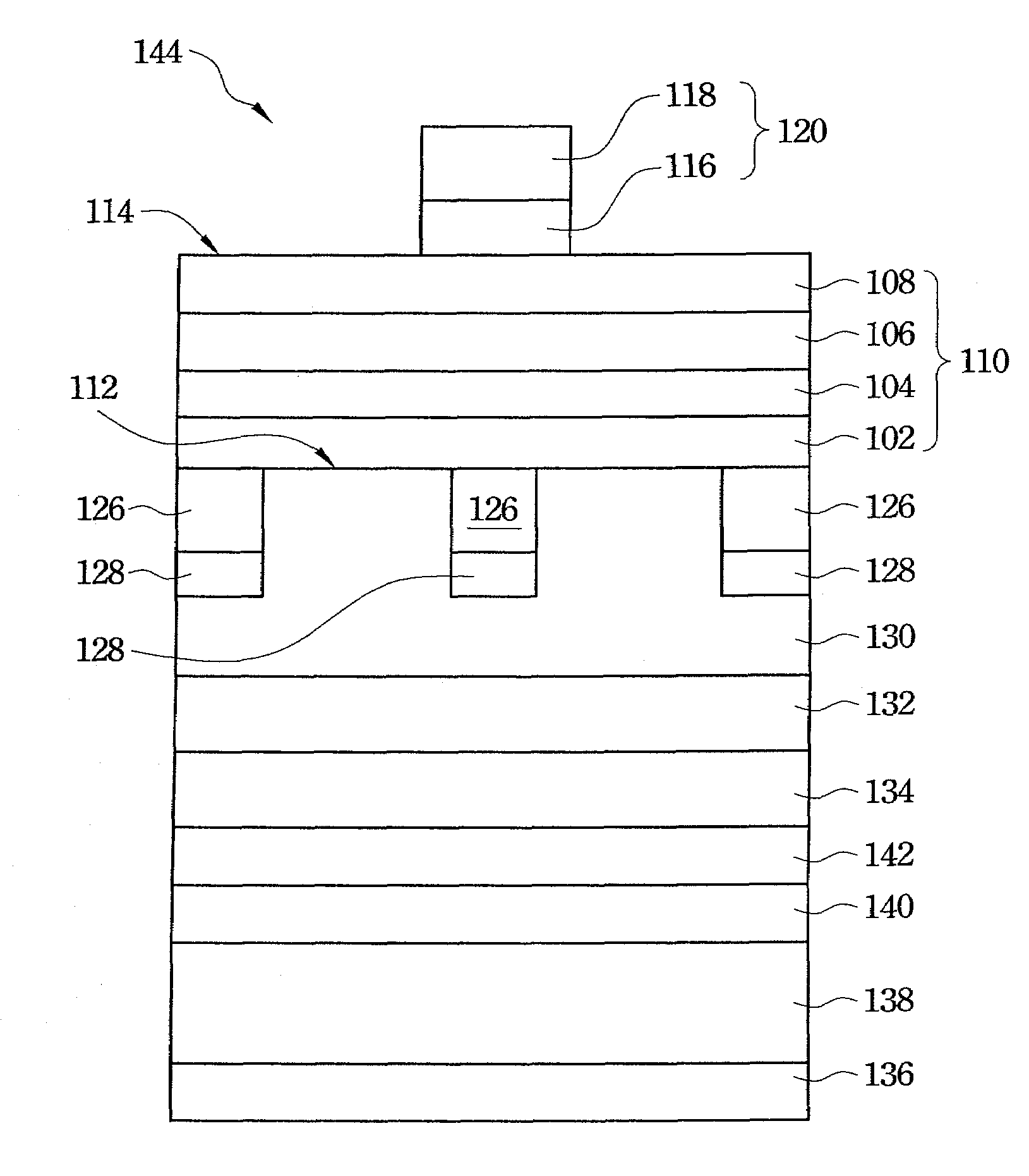
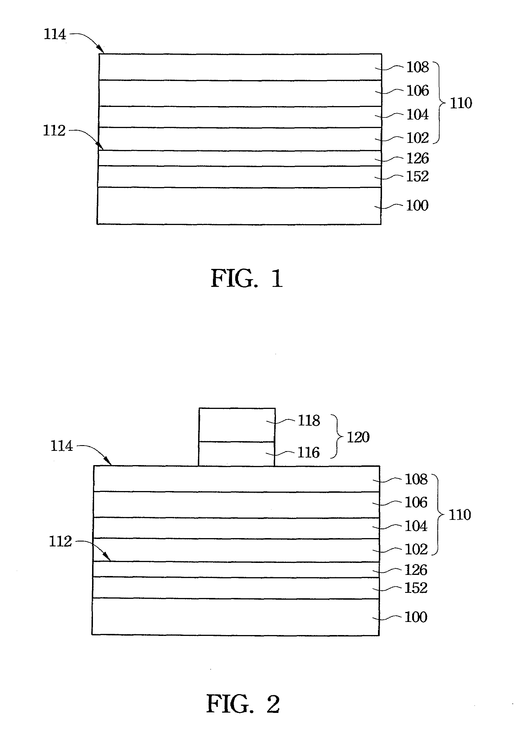
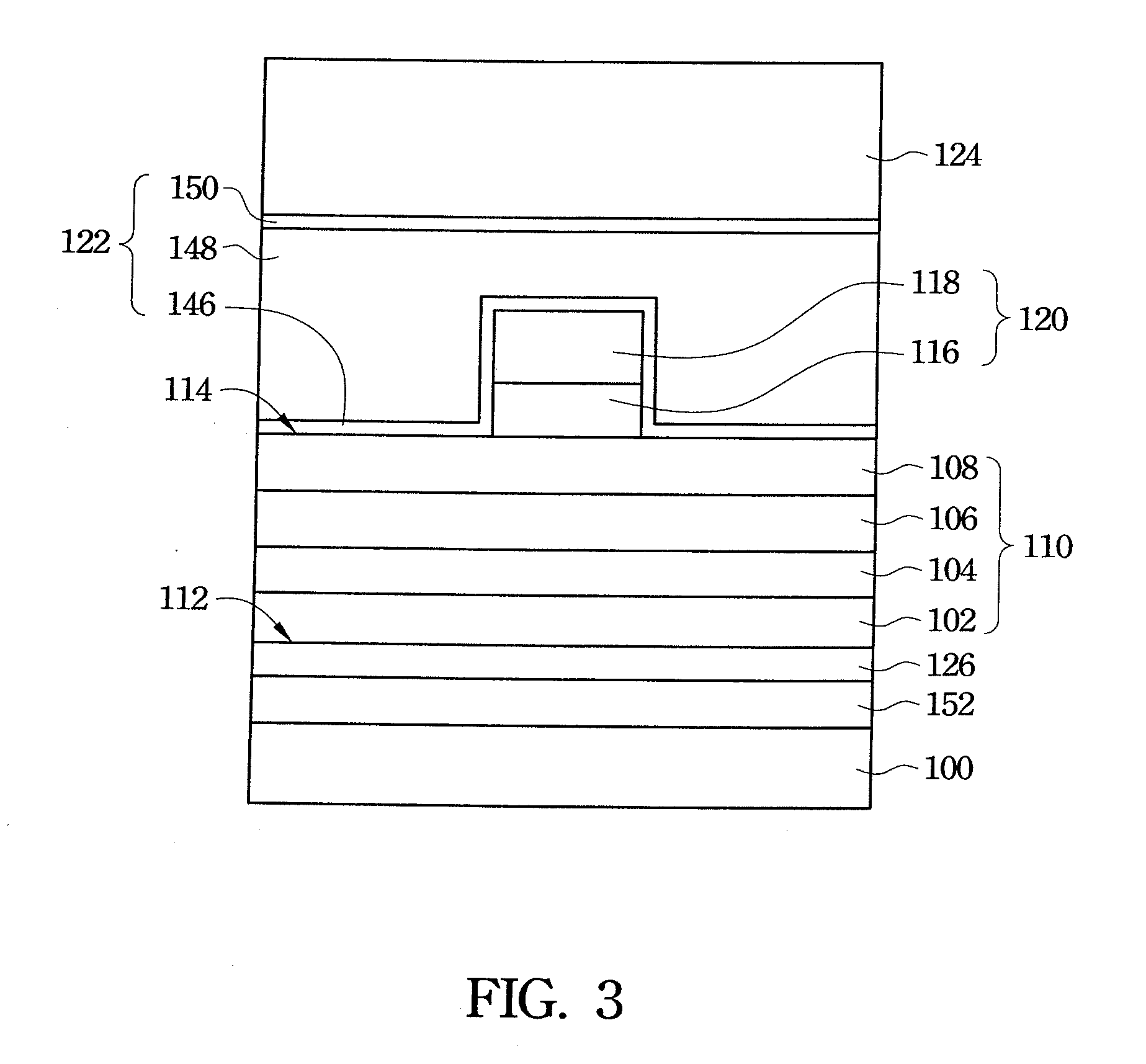
[0018]FIG. 1 through FIG. 8 are schematic flow diagrams showing the high efficiency light-emitting diode manufacturing process in accordance with a preferred embodiment of the present invention. In an exemplary embodiment of the present invention, in the fabrication of a light-emitting diode device, a growth substrate 100 is provided, and an etching stop layer 152 is directly grown on a surface of the growth substrate 100 by, for example, a deposition method. A first conductivity type ohmic contact layer 126 is formed on the etching stop layer 152, wherein a material of the f...


PUM

PropertyMeasurementUnit
bonding temperatureaaaaaaaaaa
temperatureaaaaaaaaaa

Abstract

A high efficiency light-emitting diode and a method for manufacturing the same are described. The high efficiency light-emitting diode comprises: a permanent substrate; a first contact metal layer and a second contact metal layer respectively deposed on two opposite surfaces of the permanent substrate; a bonding layer deposed on the second contact metal layer; a diffusion barrier layer deposed on the bonding layer, wherein the permanent substrate, the bonding layer and the diffusion barrier layer are electrically conductive; a reflective metal layer deposed on the diffusion barrier layer; a transparent conductive oxide layer deposed on the reflective metal layer; an illuminant epitaxial structure deposed on the transparent conductive oxide layer, wherein the illuminant epitaxial structure includes a first surface and a second surface opposite to the first surface; and a second conductivity type compound electrode pad deposed on the second surface of the illuminant epitaxial structure.

Description

RELATED APPLICATIONS[0001]This application claims priority to Taiwan Application Serial Number 95150033, filed Dec. 29, 2006, which is herein incorporated by reference.FIELD OF THE INVENTION[0002]The present invention relates to a light-emitting diode (LED) and a method for manufacturing the same, and more particularly, to a high efficiency light-emitting diode and a method for manufacturing the same.BACKGROUND OF THE INVENTION[0003]In the fabrication of light-emitting diodes, group III-V compound semiconductors, such as GaP, GaAsP, GaInP, AlGaAs, AlGaP and AlGaInP, are common. Typically, a material of a growth substrate of a conventional light-emitting diode adopts N-type gallium arsenide (GaAs). The growth substrate composed of N-type GaAs can absorb light, so that most of the photons produced by the active layer of the light-emitting diode while being emitted towards the growth substrate are absorbed by the growth substrate, thus seriously affecting the light emitting efficiency ...

Claims


Application Information

Patent Timeline
Patent Type & Authority Applications(United States)
IPC IPC(8): H01L33/00H01L33/14H01L33/30H01L33/40H01L33/42
CPCH01L33/0079H01L33/14H01L33/60H01L33/405H01L33/42H01L33/30H01L33/0093
Inventor HON, SCHANG-JING
Owner EPISTAR CORP
Why Eureka
Try Eureka