Semiconductor radiation detector and radiation detection equipment

a radiation detector and semiconductor technology, applied in the direction of electrical equipment, semiconductor devices, radiation controlled devices, etc., can solve the problems detector increase, and crystal dislocation liable to occur disadvantageously in the semiconductor crystal, so as to prevent the reduce the hardness, and prevent the effect of deterioration of the detection characteristic of the semiconductor radiation detector

Inactive Publication Date: 2008-07-03
HITACHI LTD
View PDF5 Cites 16 Cited by
  • Summary
  • Abstract
  • Description
  • Claims
  • Application Information

AI Technical Summary

Benefits of technology

[0008]Accordingly, it is an object of this invention to solve this problem and provide a semiconductor radiation detector and a radiation detection equipment capable of suitably preventing the deterioration of the detection characteristic.
[0009]In order to solve the problem described above, according to this invention, there is provided a semiconductor radiation detector and a radiation detection equipment, wherein at least one of the cathode electrode and the anode electrode includes a plurality of metals stacked in layers with the first layer being formed of Pt or Au and the second layer of a metal such as In lower in hardness than the metal of the first layer. With this configuration, in the assembly process of the semiconductor radiation detector, In of the second layer functions as a buffer material against the first layer of Pt or Au harder than In, and the pressure of bonding the electrode plate through the electroconductive adhesive is suitably alleviated. As a result, the semiconductor crystal develops no crystal dislocation and the deterioration of the detection characteristic of the semiconductor radiation detector is suitably prevented.
[0010]Also, in the case where the element In contained in the second layer is formed by electroless plating method, the semiconductor crystal is not exposed to a high temperature in forming t

Problems solved by technology

In the case where the electrode plate is bonded under pressure as described above in the process of assembling the semiconductor radiation detector, a crystal dislocation is liable to occur disadvantageously in the semiconductor crystal.
The oc

Method used


Image

  • Semiconductor radiation detector and radiation detection equipment
  • Semiconductor radiation detector and radiation detection equipment
  • Semiconductor radiation detector and radiation detection equipment

Examples


first embodiment

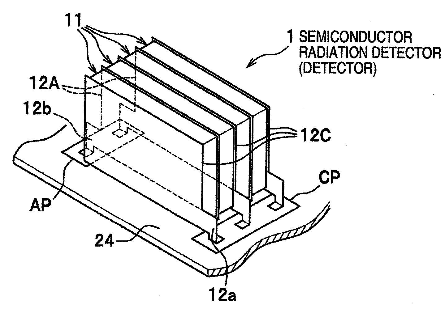
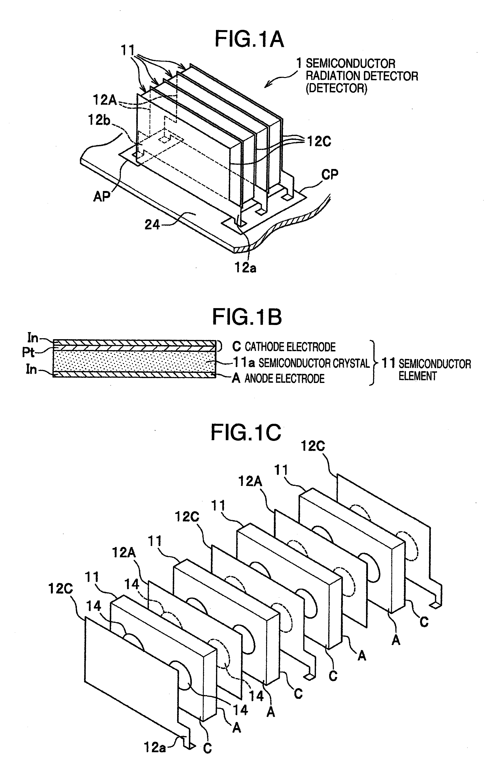
[0030]The semiconductor radiation detector (hereinafter referred to simply as the detector) 1 according to this embodiment, as shown in FIG. 1A, is a stack structure including four semiconductor elements 11, and electrode plates 12C, 12A arranged between and at the ends of the semiconductor elements 11.

[0031]The semiconductor elements 11, as shown in FIG. 1B, each have a semiconductor crystal 11a formed in the shape of a flat plate, and have a thin-film electrode formed on each entire side surface thereof. Each semiconductor element 11 is formed with a cathode electrode (hereinafter referred to as the cathode) C on one surface thereof and an anode electrode (hereinafter referred to as the anode) A on the other surface thereof.

[0032]The semiconductor crystal 11a constitutes an area for generating the charge by interaction with the radiation (γ ray, etc.), and is formed by slicing the single crystal of CdTe, CdZnTe or GaAs. According to this embodiment, each semiconductor crystal 11a ...

second embodiment

[0086]A detector according to a second embodiment of the invention is explained. The detector 1A according to this embodiment, as shown partially in FIG. 11, is different from the first embodiment in that both the electrodes of the cathode C and the anode A are in a double stack structure, each with the first layer of Pt and the second layer of In. Incidentally, the semiconductor crystal 11a is in the shape of a tabular rectangle similar to the first embodiment.

[0087]Now, the fabrication process of the semiconductor element 11′ having the cathode C and the anode A of this structure is explained.

[0088]First, Pt is deposited to the thickness of about 50 nm by the electroless plating method on the two surfaces of the semiconductor crystal 11a thereby to form the first layer of the cathode C and the anode A.

[0089]After that, In is deposited to the thickness of about 100 nm by the electroless plating method on the first layer of the cathode C and the anode A thus formed thereby to form t...


PUM


Abstract

A semiconductor radiation detector and a radiation detection equipment capable of suitably preventing the deterioration of the detection characteristics are disclosed. The semiconductor radiation detector 1 includes a semiconductor crystal 11a formed of at least one of CdTe, CdZnTe, GaAs and TlBr held between the electrodes of a cathode C and an anode A. At least one of the electrodes is a stack structure including a plurality of metals. The first layer is formed of Pt or Au, and the second layer is formed of a metal lower in hardness than Pt or Au, as the case may be, of the first layer. The second layer of In, for example, is formed by the electroless plating method. Also, a metal may be further stacked on the second layer.

Description

BACKGROUND OF THE INVENTION[0001]This invention relates to a semiconductor radiation detector and a radiation detection equipment.[0002]In recent years, the nuclear medicine diagnosis device has been widely used as a radiation detection equipment using the radiation measurement technique. Typical equipment include a positron emission tomography equipment (PET equipment), a single photon emission computed tomography equipment (SPECT equipment) and a gamma-camera equipment. The radiation detector mainly used in these equipments is a combination of a scintillator and a photomultiplier. A technique using the semiconductor radiation detector configured of the semiconductor crystal such as CdTe (cadmium telluride), CdZnTe (cadmium-zinc-tellurium), GaAs (gallium arsenide) or TlBr (thallium bromide) is closely watched as a radiation detector for detecting the radiation such as γ ray. The semiconductor radiation detector is configured to convert the charge generated by interaction between th...

Claims


Application Information

Patent Timeline
IPC IPC(8): H01L27/146
CPCH01L27/1446H01L31/0224H01L31/02966Y02E10/544H01L31/1832H01L31/1844H01L31/03046
Inventor KOMINAMI, SHINYASEINO, TOMOYUKI
Owner HITACHI LTD
Why Eureka
Try Eureka