Packing board for electronic device, packing board manufacturing method, semiconductor module, semiconductor module manufacturing method, and mobile device

a technology for electronic devices and manufacturing methods, applied in semiconductor devices, semiconductor/solid-state device details, electrical apparatus, etc., can solve the problems of reducing the reliability of the semiconductor device, and reducing the size reduction by narrowing the gap between electrodes. the effect of improving the reliability of the semiconductor modul

Inactive Publication Date: 2008-07-03
SANYO ELECTRIC CO LTD
View PDF4 Cites 11 Cited by
  • Summary
  • Abstract
  • Description
  • Claims
  • Application Information

AI Technical Summary

Benefits of technology

[0007]In this background, a general purpose of the present invention is to provide a manufacturing technology capable of improving the reliability of a semiconductor module having a via contact connected to an electrode par...

Problems solved by technology

However, efforts for size reduction by narrowing the gap between electrodes have been successful only to a limited degree due to the constraints imposed by the size of solder bumps and solder bridges produced.
However, formation of an aperture on an electrode pad by laser irradiation, as is conventionally done, involves a disadvantage in that a semiconductor device is damaged via the electrode pad due to the heat from laser, and the reliability of the semiconductor device is lowered accordingly.
While the above-mentioned method can mitigate the effect from the heat produced by laser irradiation, the electrode pad, which is ...

Method used


Image

  • Packing board for electronic device, packing board manufacturing method, semiconductor module, semiconductor module manufacturing method, and mobile device
  • Packing board for electronic device, packing board manufacturing method, semiconductor module, semiconductor module manufacturing method, and mobile device
  • Packing board for electronic device, packing board manufacturing method, semiconductor module, semiconductor module manufacturing method, and mobile device

Examples


first embodiment

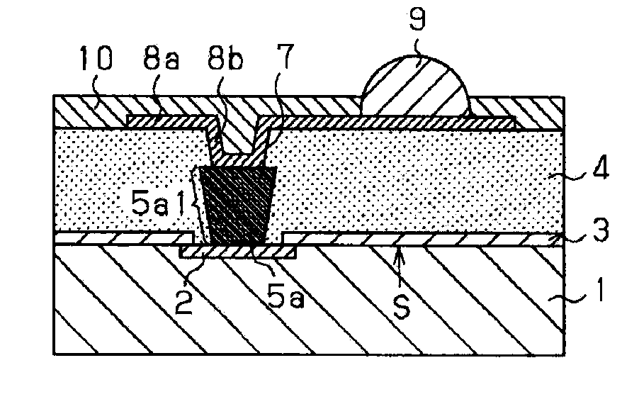
[0036]FIG. 1 is a schematic section showing the structure of a semiconductor module according to the first embodiment. A description will now be given of the semiconductor module according to the first embodiment with reference to FIG. 1.

[0037]A semiconductor substrate 1 is embodied by, for example, a p-type silicon substrate. A semiconductor device (not shown) is formed on the upper surface S (mounting surface) thereof by using a well-known technology. An electrode 2 for the semiconductor device is formed on the surface S (particularly, the periphery thereof). A protective film 3 is formed on at least a part of the surface of the semiconductor substrate 1 so as to expose a certain region of the electrode 2. In order to secure a large gap between the electrodes 2 on the surface S of the semiconductor substrate 1, an insulating layer 4 is formed on the electrode 2 and the protective film 3, and a rewiring pattern 8a is formed on the layer 4. Connection between the electrode 2 and the...

second embodiment

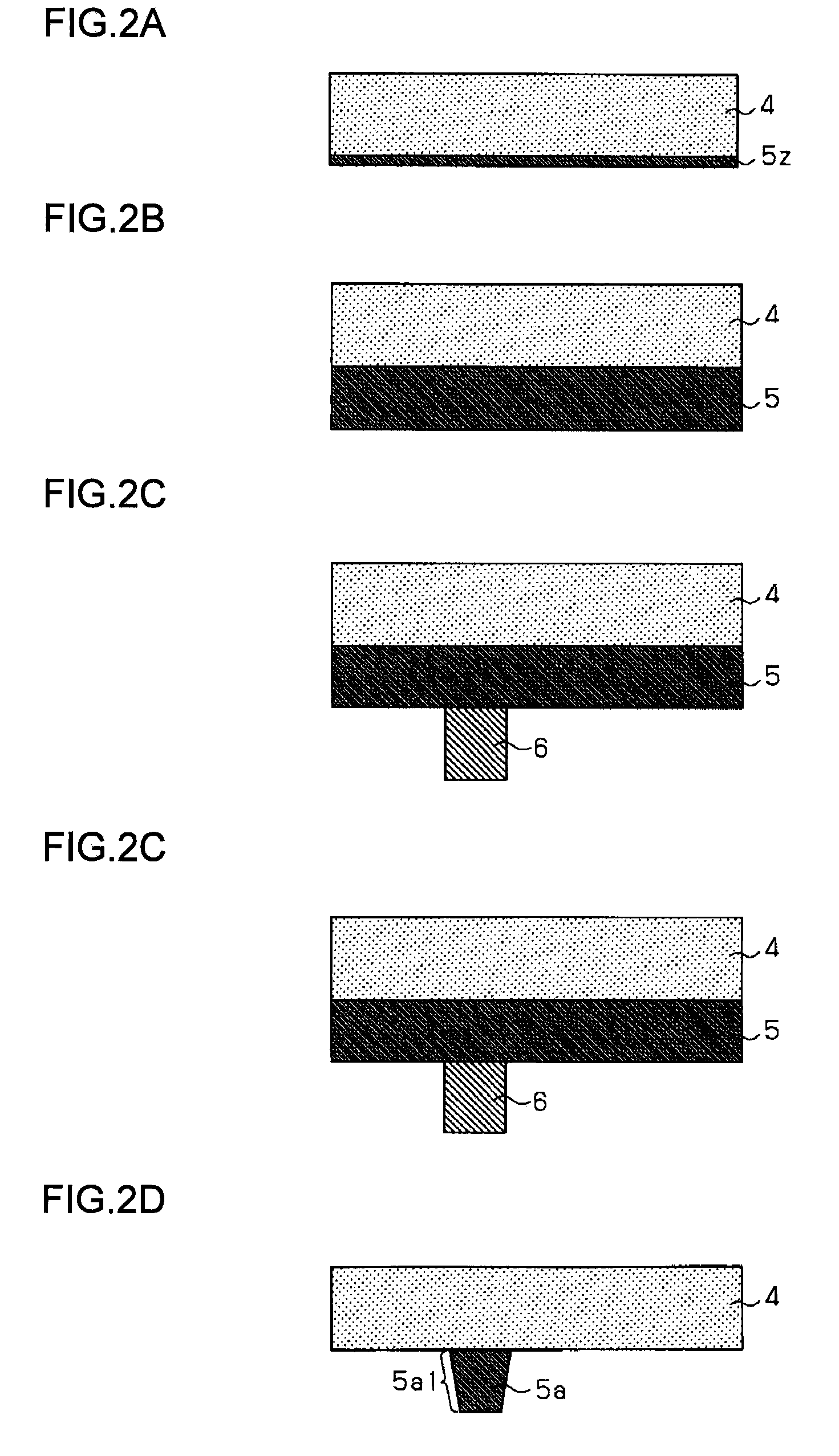
[0063]FIG. 4 is a schematic section showing the structure of a semiconductor module according to the second embodiment. A difference from the first embodiment is that a conductive bump 5b is formed to have a side part 5b1 which is progressively smaller in diameter (dimension) toward the via contact 8b and away from the electrode 2, i.e., the side part 5b1 which is progressively larger in diameter (dimension) toward the electrode 2 and away from the via contact 8b. The other aspects of the second embodiment are the same as the corresponding aspects of the first embodiment.

[0064]More specifically, the conductive bump 5b comprises a metal such as copper (Cu) and embedded in the insulating layer 4 so as to be in contact with the exposed surface of the electrode 2. The height of the conductive bump 5b is about 50 μm. The conductive bump 5b is formed as an inverted truncated cone having an inverted trapezoidal cross section, and is provided with an end part parallel with the contact surfa...

third embodiment

[0081]Recently, with the miniaturization and high performance of electronic appliances, there is a demand for reduction of the size of semiconductor modules used in electronic appliances. To achieve this, narrow-gap electrodes for external connection of semiconductor modules are essential. However, efforts for size reduction by narrowing the gap between electrodes have been successful only to a limited degree due to the constraints imposed by the size of solder bumps and solder bridges produced. Recently, there are attempts to relocate the electrodes by routing lines in a semiconductor module in an effort to overcome the limitation. For relocation, a metal plate may be half-etched so that a resultant projection is used as an electrode or a via, a semiconductor module may be mounted on the metal plate via an insulating layer of, for example, epoxy resin, and the electrode for external connection for the semiconductor module may be connected to the projection.

[0082]For improvement of ...


PUM


Abstract

A manufacturing technology is provided capable of improving the reliability of a semiconductor module having a via contact connected to an electrode part of a semiconductor device. A conductive bump is formed on an insulating layer such that the end of the conductive bump is in contact with an electrode of a semiconductor substrate. By pressure-molding the assembly using a press machine, the semiconductor substrate, the conductive bump, and the insulating layer are integrated. With this, the conductive bump is allowed to embed itself in the insulating layer while maintaining contact with the electrode. The insulating layer is subject to laser irradiation from above so as to form an aperture exposing the conductive bump. Subsequently, the upper surface of the insulating layer and the interior surface of the aperture are plated with copper by electroless plating and electroplating so as to form a copper plating layer, and a via contact is formed in the aperture so as to coat the inner wall of the aperture.

Description

CROSS-REFERENCE TO RELATED APPLICATIONS[0001]This application is based upon and claims the benefit of priority from the prior Japanese Patent Applications No. 2006-337708, filed Dec. 15, 2006, Japanese Patent Application No. 2006-343036 filed on Dec. 20, 2006, Japanese Patent Application No. 2007-314241, filed Dec. 5, 2007 and Japanese Patent Application No. 2007-314240, filed Dec. 5, 2007, the entire contents of which are incorporated herein by reference.BACKGROUND OF THE INVENTION[0002]1. Field of the Invention[0003]The present invention relates to packing boards adapted to mount an electronic device, semiconductor modules and methods of manufacturing the same.[0004]2. Description of the Related Art[0005]Recently, with the trend toward miniaturization and high performance of electronic devices, there is a demand for reduction of the size of semiconductor devices used in electronic devices. To achieve this, narrow-gap electrodes for external connection for semiconductor devices are...

Claims


Application Information

Patent Timeline
IPC IPC(8): H01L21/50H01L23/52
CPCH01L23/3114H01L2224/0401H01L24/11H01L24/12H01L2224/0231H01L2224/02313H01L2224/13022H01L2224/13099H01L2224/13147H01L2224/16H01L2924/01002H01L2924/01005H01L2924/01013H01L2924/01015H01L2924/01029H01L2924/01074H01L2924/01078H01L2924/01079H01L2924/01082H01L2924/01006H01L2924/01033H01L2924/014H01L2224/02319H01L2224/02333H01L23/525H01L2924/351H01L2924/00
Inventor NAKASATO, MAYUMISHIBATA, KIYOSHIOKAYAMA, YOSHIOUSUI, RYOSUKEMIZUHARA, HIDEKI
Owner SANYO ELECTRIC CO LTD
Why Eureka
Try Eureka