Impurity introducing apparatus and impurity introducing method

a technology which is applied in the field of impurity introducing apparatus and impurity introducing method, can solve the problems of inability to produce the advantage of amorphization, and inability to accurately control the characteristic and amount of impurity to be doped into a semiconductor thin film. to achieve the effect of accurate manufacturing of semiconductor

Inactive Publication Date: 2008-07-10
PANASONIC CORP
View PDF24 Cites 3 Cited by
  • Summary
  • Abstract
  • Description
  • Claims
  • Application Information

AI Technical Summary

Benefits of technology

[0068]According to the invention, a substance to retain electrically positive and negative characteristics is prevented from being mixed at a certain step in an introduction of an impurity into a semiconductor substrate in a manufacture of a semiconductor apparatus, thereby contributing to an accurate manufacture of the semiconductor apparatus. More specifically, a method of distinguishing an impurity is shown and a solution can be carried out in consideration of the circumstances such as a cost performance in a manufacturing factory.

Problems solved by technology

As a result, it is impossible to accurately control the characteristic and amount of the impurity to be doped into a semiconductor thin film.
For this reason, the plasma doping method is used with difficulties in a manufacture of a semiconductor on which the characteristic greatly depends based on a very small difference in an amount.
More specifically, even if a large amount of He is irradiated for a long period of time in a He ion implantation through a conventional beam line ion implantation, the silicon single crystal substrate cannot be amorphized.
However, it was impossible to produce the advantage of the amorphization.

Method used


Image

  • Impurity introducing apparatus and impurity introducing method
  • Impurity introducing apparatus and impurity introducing method
  • Impurity introducing apparatus and impurity introducing method

Examples


first embodiment

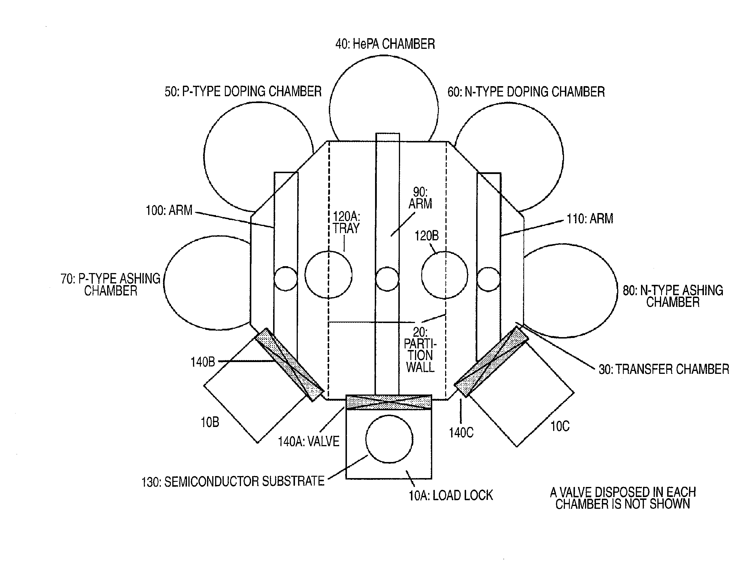
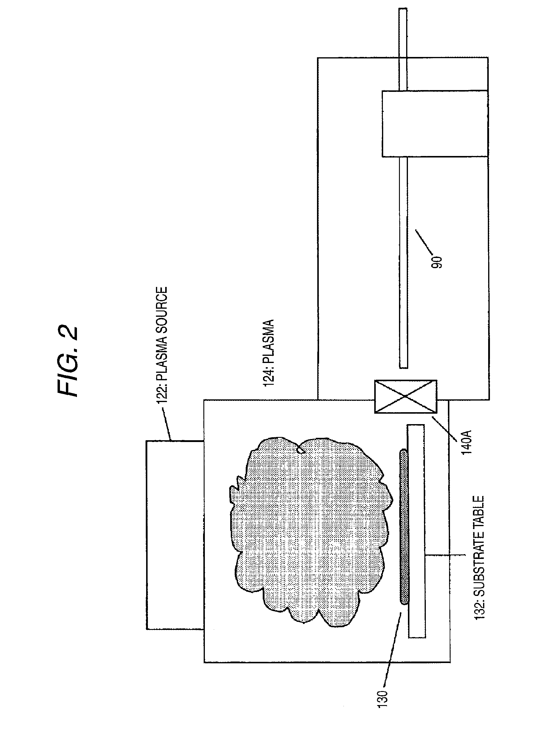
[0094]An embodiment according to the invention will be described with reference to FIG. 1. A plasma doping apparatus is an example in which a plasma in a vacuum state is utilized. If it is possible to make the best of features of various plasmas, the plasma in the vacuum state is not restricted.

[0095]The example features that a He plasma amorphization (HePA) is carried out and impurity doping is then performed.

[0096]In the invention, in an apparatus having a structure which will be described below, three load locks 10 are provided and five plasma chambers are disposed in a transfer chamber 30 having a structure which can be separated through a partition wall 20 depending on uses. The five plasma chambers are constituted by a HePA chamber 40, a P-type doping chamber 50 using B2H6, an N-type doping chamber 60 using PH3, a P-type ashing chamber 70 for removing a photoresist on a semiconductor substrate subjected to P-type doping, and an N-type ashing chamber 80 for removing a photoresi...

second embodiment

[0112]A second embodiment according to the invention will be described with reference to FIG. 3.

[0113]In the invention, description will be given to an example in which HePA and doping are carried out in the same chamber.

[0114]First of all, an apparatus will be described.

[0115]Load locks 10B and 10C are used for P and N types, respectively.

[0116]Four plasma chambers are disposed in a transfer chamber 30. The four plasma chambers are constituted by a P-type doping chamber 50 using B2H6, an N-type doping chamber 60 using PH3, a P-type ashing chamber 70 for removing a photoresist on a semiconductor substrate subjected to P-type doping, and an N-type ashing chamber 80 for removing a photoresist on a semiconductor substrate subjected to N-type doping. In order to deliver the semiconductor substrate among the load lock, the transfer chamber, and the plasma chamber, a robot arm is disposed. The robot arm is designed to be freely rotatable at 360 degrees. In this case, three types of a P-ty...

third embodiment

[0132]A third embodiment according to the invention will be described with reference to FIG. 4. A plasma doping apparatus is an example in which a plasma in a vacuum state is utilized. It is sufficient to make the best of features of various plasmas and the plasma in the vacuum state is not restricted.

[0133]The embodiment features that an apparatus group for carrying out a He plasma amorphization (HePA), and then, impurity doping and removing a photoresist is arranged intentionally to efficiently execute a serial step. Referring to the delivery of the semiconductor substrate, however, by using wafer delivering mechanisms managed highly in a semiconductor manufacturing factory and their managing functions, it is sufficiently possible to exhibit a serial function by the presence of an apparatus group capable of fulfilling the same function even if a great distance is made therebetween or they are not stored in one enclosure for reasons of an arrangement in the factory. In the extreme,...


PUM

PropertyMeasurementUnit
thicknessaaaaaaaaaa
thicknessaaaaaaaaaa
electricalaaaaaaaaaa

Abstract

It is an object to prevent functions expected originally from being unexhibited when impurities to be introduced into a solid sample are mixed with each other, and to implement plasma doping with high precision. In order to distinguish impurities which may be mixed from impurities which should not be mixed, first of all, an impurity introducing mechanism of a core is first distinguished. In order to avoid a mixture of the impurities in very small amounts, a mechanism for delivering a semiconductor substrate to be treated and a mechanism for removing a resin material to be formed on the semiconductor substrate are used exclusively.

Description

TECHNICAL FIELD[0001]The present invention relates to an impurity introducing apparatus and an impurity introducing method, and more particularly to a plasma doping apparatus and a plasma doping method which serve to implant an ion onto a surface of a solid sample by using a plasma.BACKGROUND ART[0002]There has been proposed a technique referred to as plasma doping in order to introduce a P-type impurity or an N-type impurity when forming a PN junction in a process for manufacturing a semiconductor such as a transistor.[0003]This serves to expose a semiconductor substrate to a plasma containing an electrically active impurity to introduce an impurity into a surface portion of the semiconductor substrate with an energy of a plasma when doping the semiconductor substrate with the impurity.[0004]Referring to a necessary impurity for a semiconductor, however, a purification or a quantitative control at an element and molecule level of the impurity is required in order to definitely give...

Claims


Application Information

Patent Timeline
Patent Type & Authority Applications(United States)
IPC IPC(8): H01L21/26
CPCH01L21/2236H01J37/32412H01L21/67167H01L21/265H01L21/02
Inventor MIZUNO, BUNJINAKAYAMA, ICHIROSASAKI, YUICHIROOKUMURA, TOMOHIROJIN, CHENG-GUOITO, HIROYUKI
Owner PANASONIC CORP
Why Eureka
Try Eureka