Semiconductor memory having function to determine semiconductor low current

Inactive Publication Date: 2008-07-17
PANASONIC SEMICON SOLUTIONS CO LTD
View PDF7 Cites 17 Cited by
  • Summary
  • Abstract
  • Description
  • Claims
  • Application Information

AI Technical Summary

Benefits of technology

[0094]Instead of comparing the current value of the first node with that of the second node, this determination device extracts the differential current between the current value of the fir

Problems solved by technology

One of the problems that recent non-volatile memories are facing is the increase in the bit line leak current due to an increase in the memory array capacity.
This is because of the increase in the number of memory cells per bit line, in addition to the increase in the leak current (bit line leak current) per memory cell, which is caused by the miniaturization process.
An increase in the bit line leak current influences the memory cell read operation, thereby detracting from the precision of the memory cell threshold value control and thus deteriorating the reliability, e.g., the data holding property.
In a verifying operation, a bit line leak current causes the system to erroneously determine the cell current by the magnitude of the leak current, thereby leading to overwriting, undererasing, etc., thus preventing the system from normally controlling the threshold value of a memory cell.
The current measurement of the test apparatus is relatively slow, taking an amount of time on the order of ms to 10 ms per an iteration of current measurement, whereby a test time generally on the order of 10 seconds is required for measuring all of the thousands o

Method used


Image

  • Semiconductor memory having function to determine semiconductor low current
  • Semiconductor memory having function to determine semiconductor low current
  • Semiconductor memory having function to determine semiconductor low current

Examples


Example

Embodiment 1

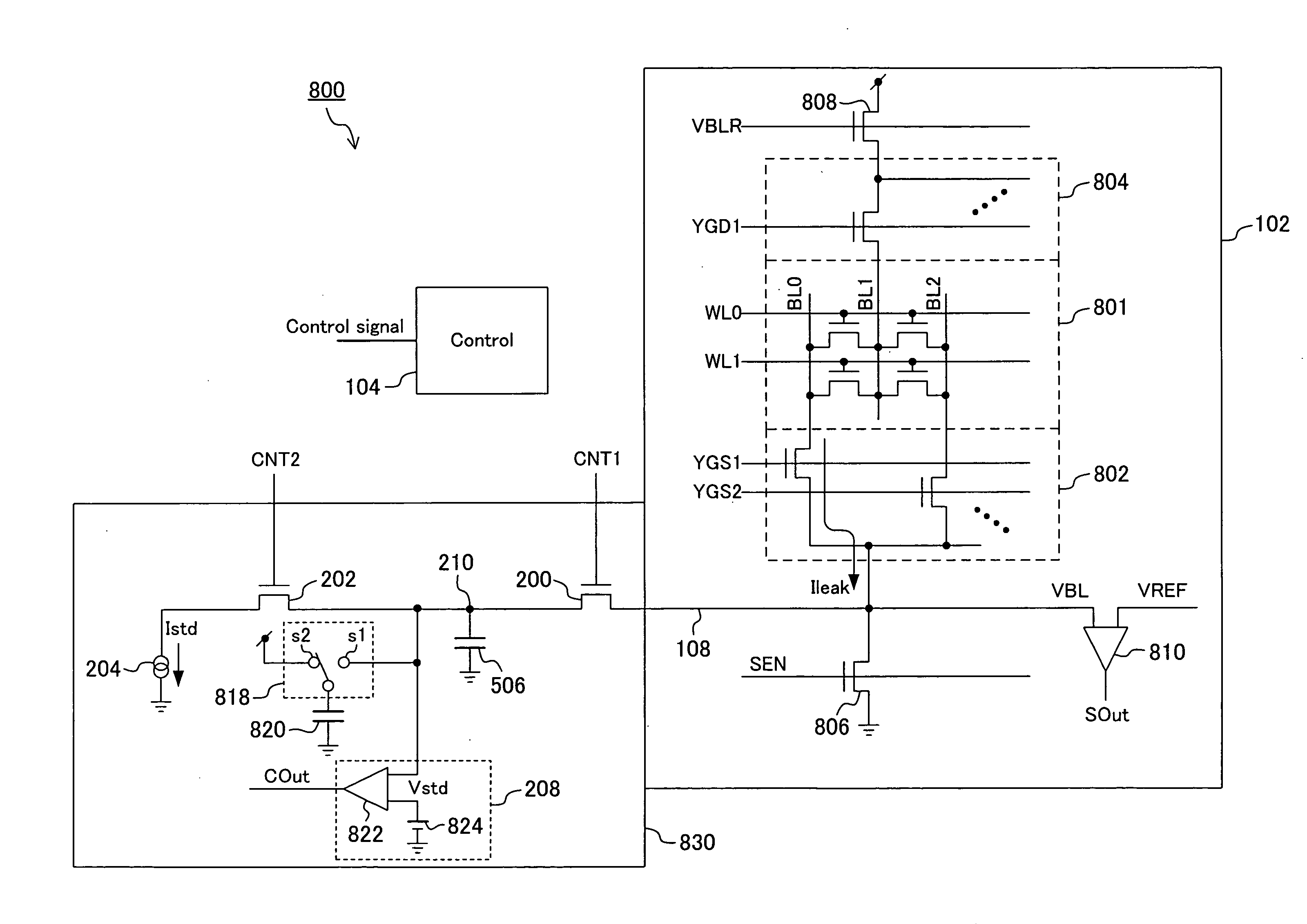
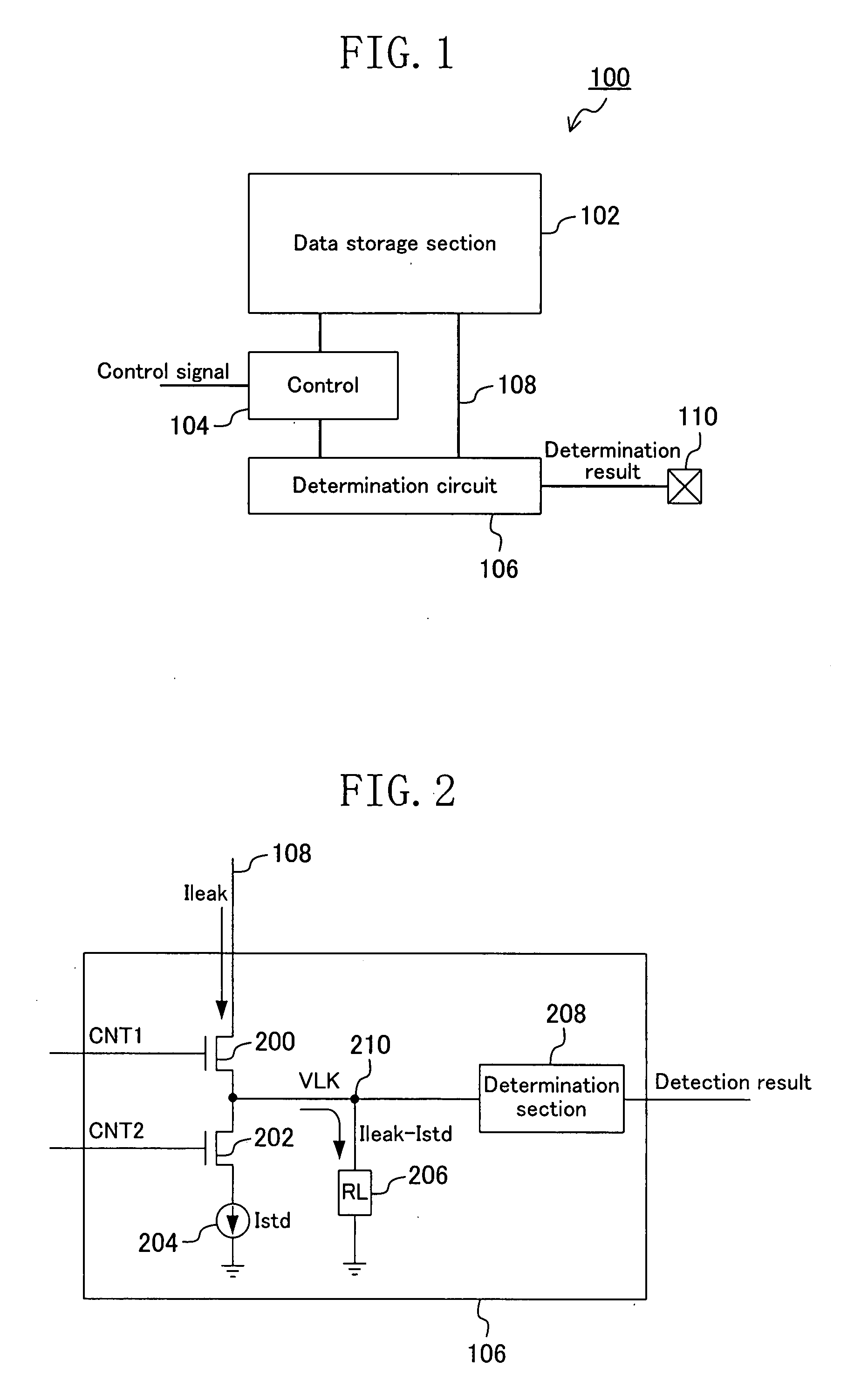
[0119]FIG. 1 is a schematic block diagram of a semiconductor memory according to Embodiment 1 of the present invention. Referring to FIG. 1, the semiconductor memory of the present embodiment is different from the conventional semiconductor memory shown in FIG. 20 in that the node 108, to which a bit line from the data storage section 102 is selectively connected, is connected to a determination circuit 106 for determining the bit line leak current, and that the leak current value determined by the determination circuit 106 is output to the external terminal 110.

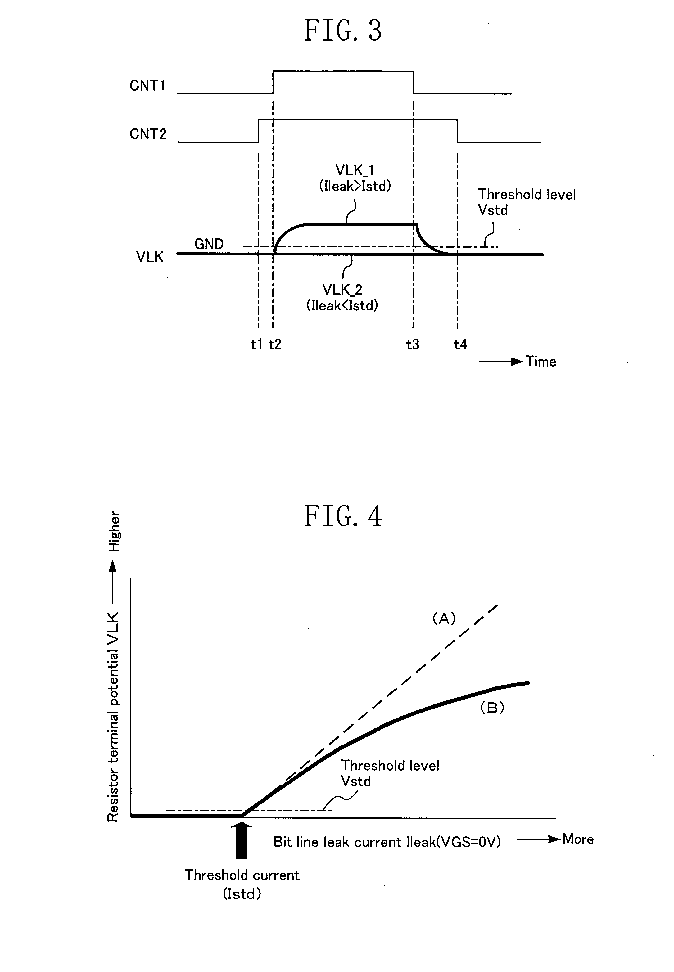
[0120]FIG. 2 shows an exemplary circuit configuration of the determination circuit 106, and FIG. 3 shows a timing diagram of the leak current determination. During the bit line leak determination operation, the bias conditions, etc., of the data storage section 102 are set to those of the leak determination mode under control of the control circuit 104, and the leak current Ileak of the selected bit line flows in...

Example

Embodiment 2

[0131]There is a demand for sub-μA current values to be used in the bit line leak determination, and there is a concern for erroneous operations due to noise when a circuit operates to make determinations on such low currents.

[0132]FIG. 5 is an exemplary circuit configuration of the determination circuit 106, in which a capacitor 506 is used to implement means for converting the differential current (Ileak−Istd) between the leak current Ileak and the threshold current Istd to a voltage, whereby erroneous operations due to noise are suppressed while reducing the layout size. The determination circuit 106 shown in FIG. 5 is different from that shown in FIG. 2 in that the capacitor 506 is the destination to which the differential current (Ileak−Istd) flows when the leak current Ileak of the selected bit line is greater than the threshold current Istd.

[0133]FIG. 6 shows a timing diagram of the leak current determination operation. As shown in FIG. 6, the control signals CNT1...

Example

Embodiment 3

[0144]The threshold voltage in the determination section 208 in Embodiments 1 and 2 is a value obtained by converting the differential current (Ileak−Istd) between the leak current Ileak and the threshold current Istd to a voltage, and the potential thereof increases off the ground potential only when the leak current Ileak is greater than the threshold current Istd. Therefore, in order to increase the determination precision, it is preferred that Vstd being the threshold level is compared with the converted voltage while setting Vstd to be as close to the ground potential as possible.

[0145]However, in order to compare a potential close to the ground potential, the determination section 208 needs to be a circuit that precisely responds to an input signal close to the ground potential. It is generally difficult to ensure a sufficient circuit operation margin with such a circuit operation with an input signal level close to the ground potential, and it is not suitable for ...


PUM


Abstract

A semiconductor memory, including a plurality of word lines, a plurality of bit lines, a plurality of memory cells provided at intersections between the plurality of word lines and the plurality of bit lines, and a sense amplifier for reading out what is stored in the memory cells, the semiconductor memory including: bit line selection means for selecting a bit line from among the plurality of bit lines; switch means for turning ON/OFF a current of the bit line selected by the bit line selection means; current generation means for generating a threshold current; means for extracting a differential current between the selected bit line current and the threshold current when a value of the selected bit line current is greater than that of the threshold current; voltage conversion means for converting the differential current to a voltage; and determination means for determining a magnitude relationship between the threshold current and the selected bit line current based on an output voltage from the voltage conversion means.

Description

CROSS REFERENCE TO RELATED APPLICATION[0001]This application claims priority under 35 U.S.C. §119 on Patent Application No. 2007-007239 filed in Japan on Jan. 16, 2007, the entire contents of which are hereby incorporated by reference.BACKGROUND OF THE INVENTION[0002]The present invention relates to a method and a device for determining a semiconductor low current (e.g., a bit line leak current in a semiconductor memory such as a flash memory).[0003]In recent years, a non-volatile memory such as a flash memory and an EEPROM employs a large-capacity memory array configuration using miniaturized memory cells.[0004]One of the problems that recent non-volatile memories are facing is the increase in the bit line leak current due to an increase in the memory array capacity. This is because of the increase in the number of memory cells per bit line, in addition to the increase in the leak current (bit line leak current) per memory cell, which is caused by the miniaturization process. An in...

Claims


Application Information

Patent Timeline
IPC IPC(8): G11C29/50
CPCG11C16/04G11C2029/5006G11C29/025G11C29/02
Inventor MORI, TOSHIKI
Owner PANASONIC SEMICON SOLUTIONS CO LTD
Why Eureka
Try Eureka