

Plasma processing apparatus and plasma processing method
- Summary
- Abstract
- Description
- Claims
- Application Information
AI Technical Summary
Benefits of technology
Problems solved by technology
Method used
Image

Examples
first embodiment
[0035]A first embodiment of the present invention will be described with reference to FIGS. 1 to 4.
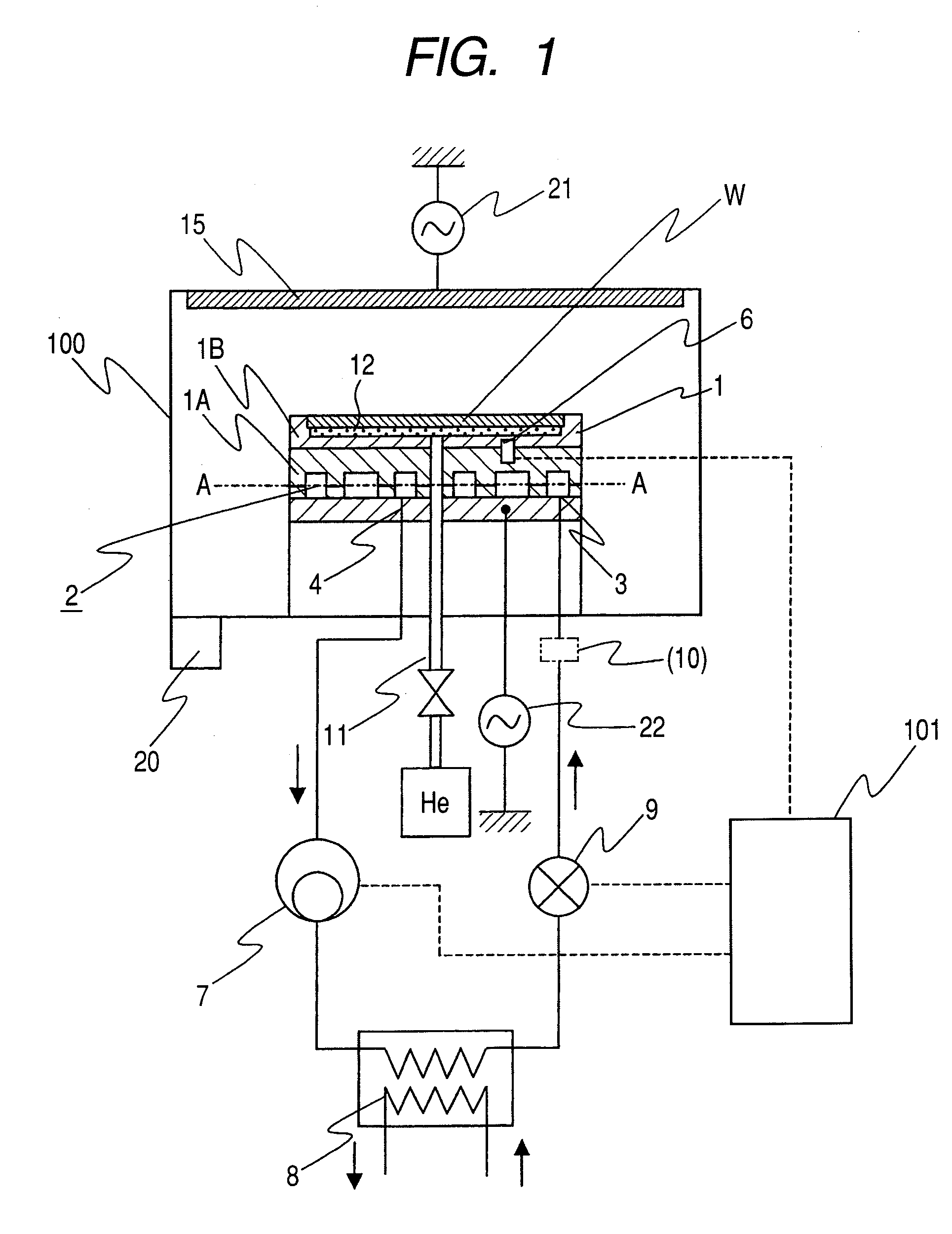
[0036]FIG. 1 is a schematic diagram showing the whole system configuration of a plasma processing apparatus that is an embodiment of the present invention. The plasma processing apparatus includes a processing chamber 100 arranged in a vacuum vessel, and a sample stage 1 having an electrostatic absorption electrode is arranged inside the processing chamber 100. The processing chamber 100 is connected to a vacuum evacuation apparatus 20 such as a vacuum pump for evacuating the inside of the processing chamber 100 for pressure reduction. An electrode plate 15 is provided on an upper portion of the processing chamber 100, and an antenna power source 21 is connected to the electrode plate 15. A gas introduction means such as a shower plate (not shown) for supplying a process gas is provided on an upper portion of the processing chamber 100.
[0037]The sample stage 1 includes a base material ...
second embodiment
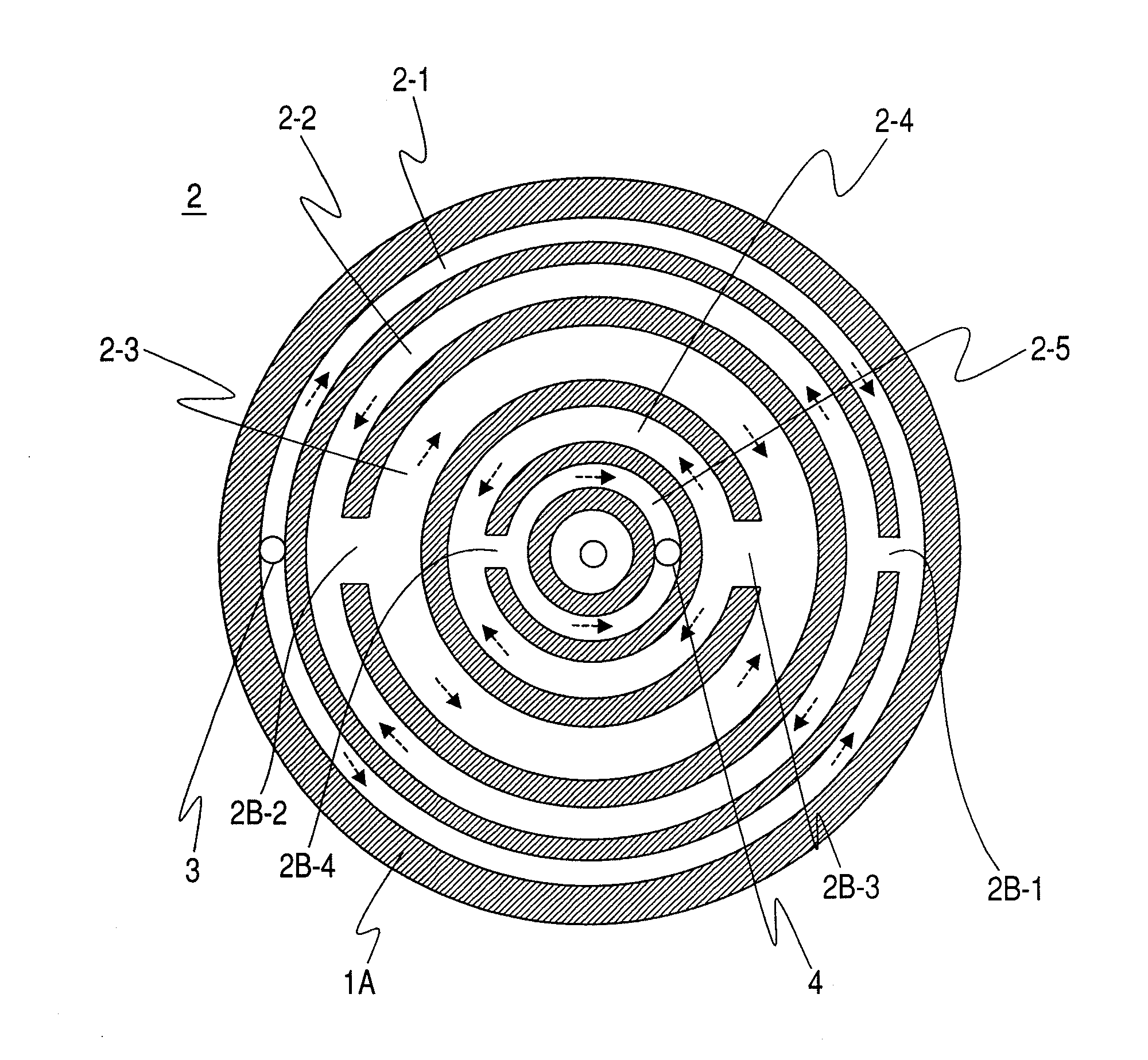
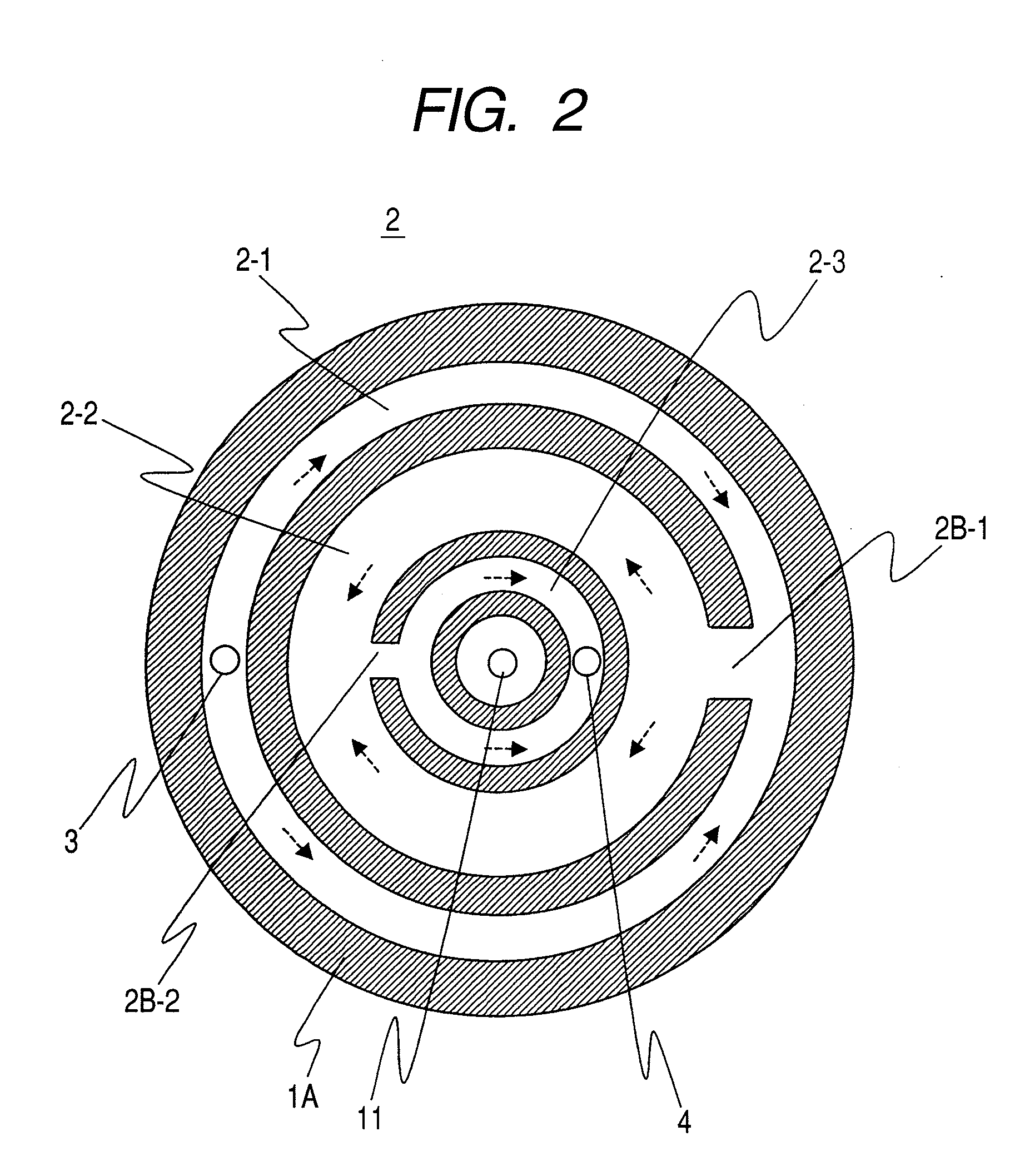
[0062]It should be noted that in the case where the temperature distribution of the sample stage 1 is uniformly controlled with more accuracy, it is advantageous that the refrigerant channel structure 2 is diversified. As a second embodiment of the present invention, an example in which the refrigerant channel structure is diversified (changed in five steps) is shown in FIG. 5. The refrigerant channel structure 2 includes five channel portions; a first channel 2-1 that is connected to the refrigerant supply port 3 and is branched into the left and right directions, a second channel 2-2 that is branched into the left and right directions through a first linkage channel 2B-1, a third channel 2-3 that is branched into the left and right directions through a second linkage channel 2B-2, a fourth channel 2-4 that is branched into the left and right directions through a third linkage channel 2B-3, and a fifth channel 2-5 that is branched into the left and right directions through a fourth...
third embodiment
[0064]In the examples shown in FIGS. 2 and 5, the placement positions of the refrigerant supply port 3 and the refrigerant outlet port 4 may be opposite. However, in this case, to take FIG. 2 as an example, the relation between the cross sections A (A1, A2, A3) of the first channel 2-1 and that of the third channel 2-3 needs to be opposite, and the relation between the cross section of the linkage channel 2B-1 and that of the linkage channel 2B-2 needs to be also opposite.
PUM
 Abstract
Description
Claims
Application Information