

Novel nanoparticle containing siloxane polymers
a technology of nanoparticles and polymers, which is applied in the direction of semiconductor devices, solid-state devices, semiconductor/solid-state device details, etc., can solve the problems of low thermal stability, the organic polymer cannot be chemically mechanically polished or etched back by dry processing without damaging the film, etc., to achieve excellent chemical resistance, low chemical adsorption behavior, and high cross-linking
- Summary
- Abstract
- Description
- Claims
- Application Information
AI Technical Summary
Benefits of technology
Problems solved by technology
Method used
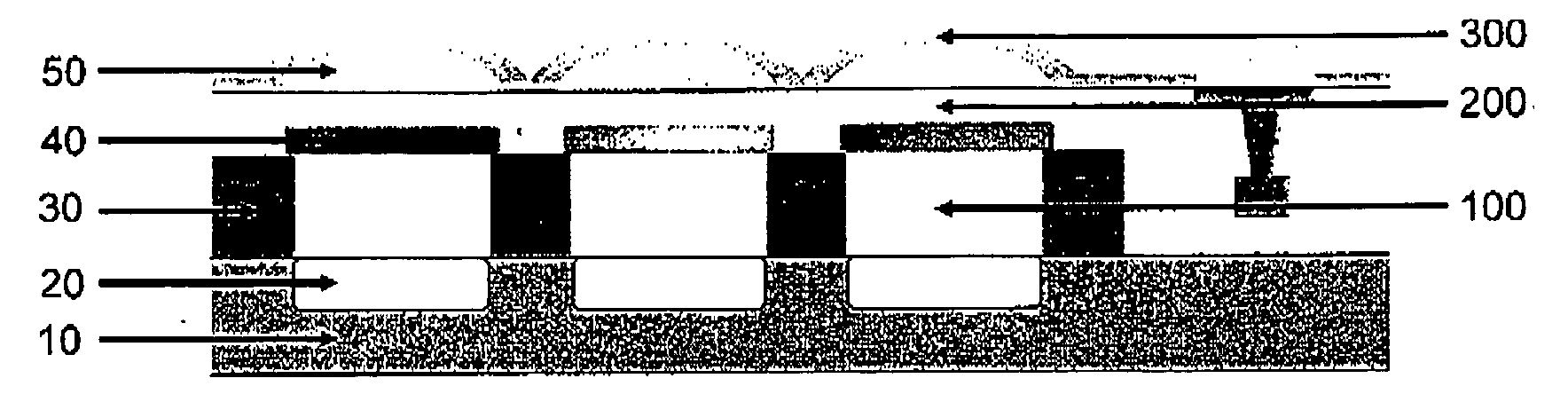
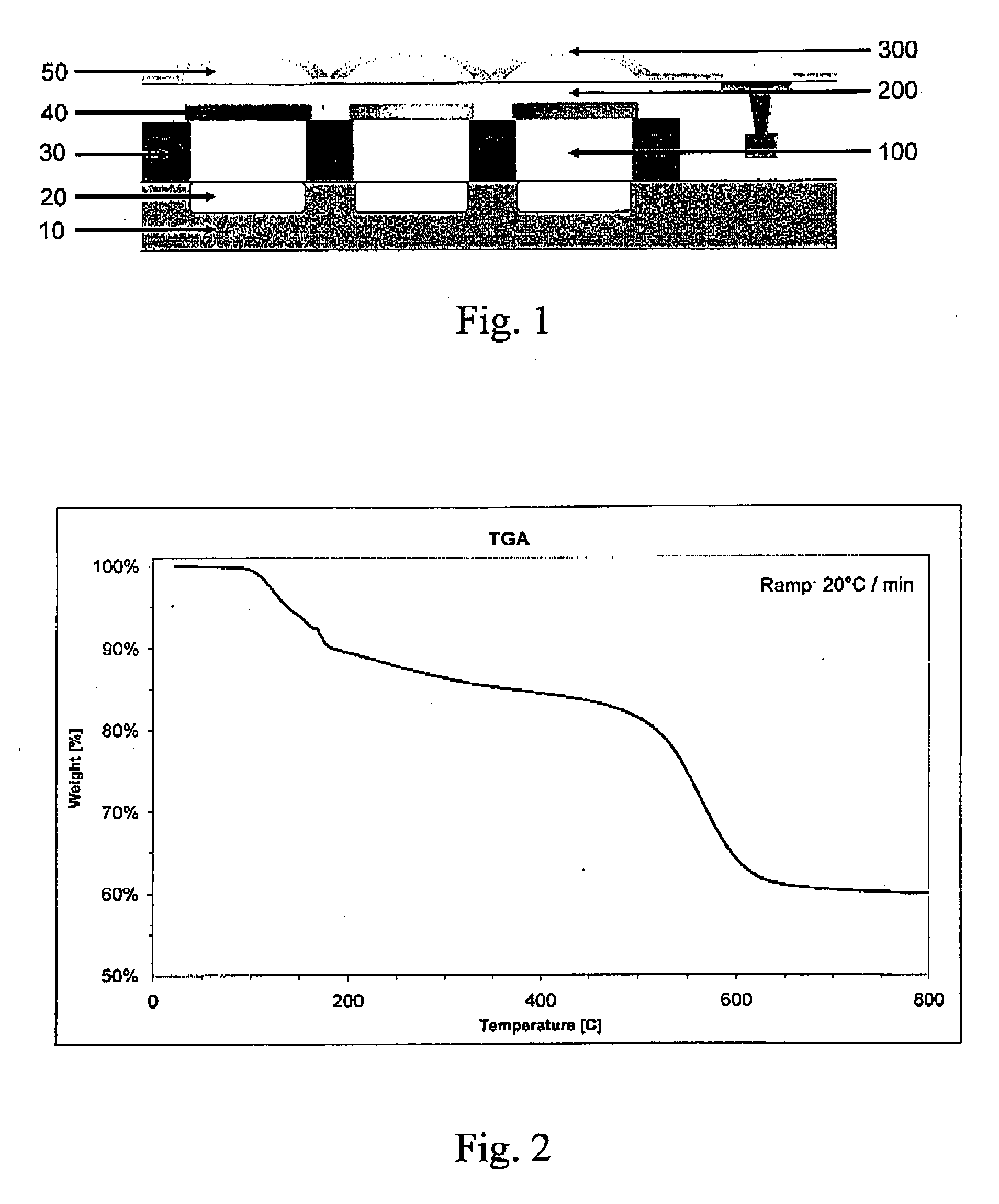
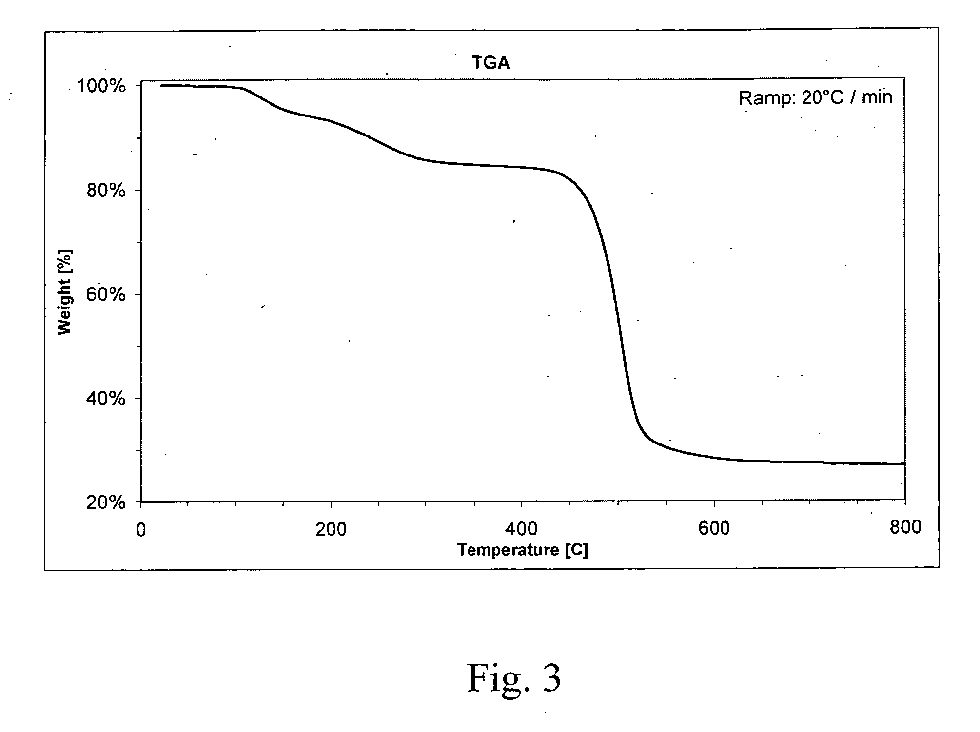
Image

Examples
example 1
1,1,1,4,4-Pentachloro-1,4-disilabutane (The Intermediate)
[0124]
[0125]Vinyltrichlorosilane (68.8 g, 426 mmol) and cobalt octacarbonyl (700 mg) were placed in a 100 mL rb flask and cooled in an ice bath to 0° C. Dichlorosilane (bp. 8° C., 44.3 g, 439 mmol) was then condensed into the flask, The system was allowed to warm up to room temperature during night. Distillation at 60 . . . 62° C. / 8 mbar gave 1,1,1,4,4-Pentachloro-1,4-disilabutane (120.8 g, 460 mmol) in 93% yield.
example 2
Tris(3,3,6,6,6-pentachloro-3,6-disilahexyl)chlorosilane
[0126]
[0127]11.00 g (0.076 mol) trivinylchlorosilane was added to a 100 ml vessel followed by 2 ml 1,1,1,4,4-pentachloro-1,4-disilabutane. The solution was heated to 80° C. and 15 μL of a 10% H2PtCl6 / IPA-solution was added. Strong exothermic reaction was observed and heat was switched off. Rest of 1,1,1,4,4-pentachloro-1,4-disilabutane was added slowly during 30 min keeping the temperature of the solution below 130° C. The total amount of 1,1,1,4,4-pentachloro-1,4-disilabutane was 61.50 g (0.234 mol, 2.6% excess). After addition heat was again switched on and solution was stirred for an hour at 110° C. After that solution was distilled yielding 47.08 g (66%) tris(3,3,6,6,6-pentachloro-3,6-disilahexyl)chlorosilane. B.p. 264° C. / <0.5 mbar.
example 3
1,1,1,4,4,7,7,7-Octachloro-1,4,7-trisilaheptane
[0128]
[0129]Vinyltrichlorosilane (16.8 g, 104 mmol) was heated to 60° C. and 100 μL 10% H2PtCl6 / IPA-solution was added. 1,1,1,4,4-pentachloro-1,4-disilabutane (20.4 g, 77.7 mmol) was added slowly during 20 min so that the temperature did not exceed 100° C. The reaction was allowed to proceed for 12 hours at 100° C., after which it was distilled under vacuum at 115-130° C. / <1 mbar. The yield was 31.5 g (74.3 mmol, 96%).
PUM
| Property | Measurement | Unit |
|---|---|---|
| particle size | aaaaa | aaaaa |
| particle size | aaaaa | aaaaa |
| thickness | aaaaa | aaaaa |
Abstract
Description
Claims
Application Information