Composition and method of preparing nanoscale thin film photovoltaic materials

Inactive Publication Date: 2008-08-14
BRICOLEUR PARTNERS LP
View PDF19 Cites 30 Cited by
  • Summary
  • Abstract
  • Description
  • Claims
  • Application Information

AI Technical Summary

Benefits of technology

[0021]Additionally, the composition may also comprise an environmental protection layer. Preferably, this layer is

Problems solved by technology

The high cost of polysilicon and resultant high cost of silicon solar cells has prevented widespread use of solar energy.
Although these materials have some of the highest efficiencies of all classes of solar cells, exceeding 15%, several steps in the production process of CIGS s

Method used


Image

  • Composition and method of preparing nanoscale thin film photovoltaic materials
  • Composition and method of preparing nanoscale thin film photovoltaic materials

Examples


example

Preparation of CIGS

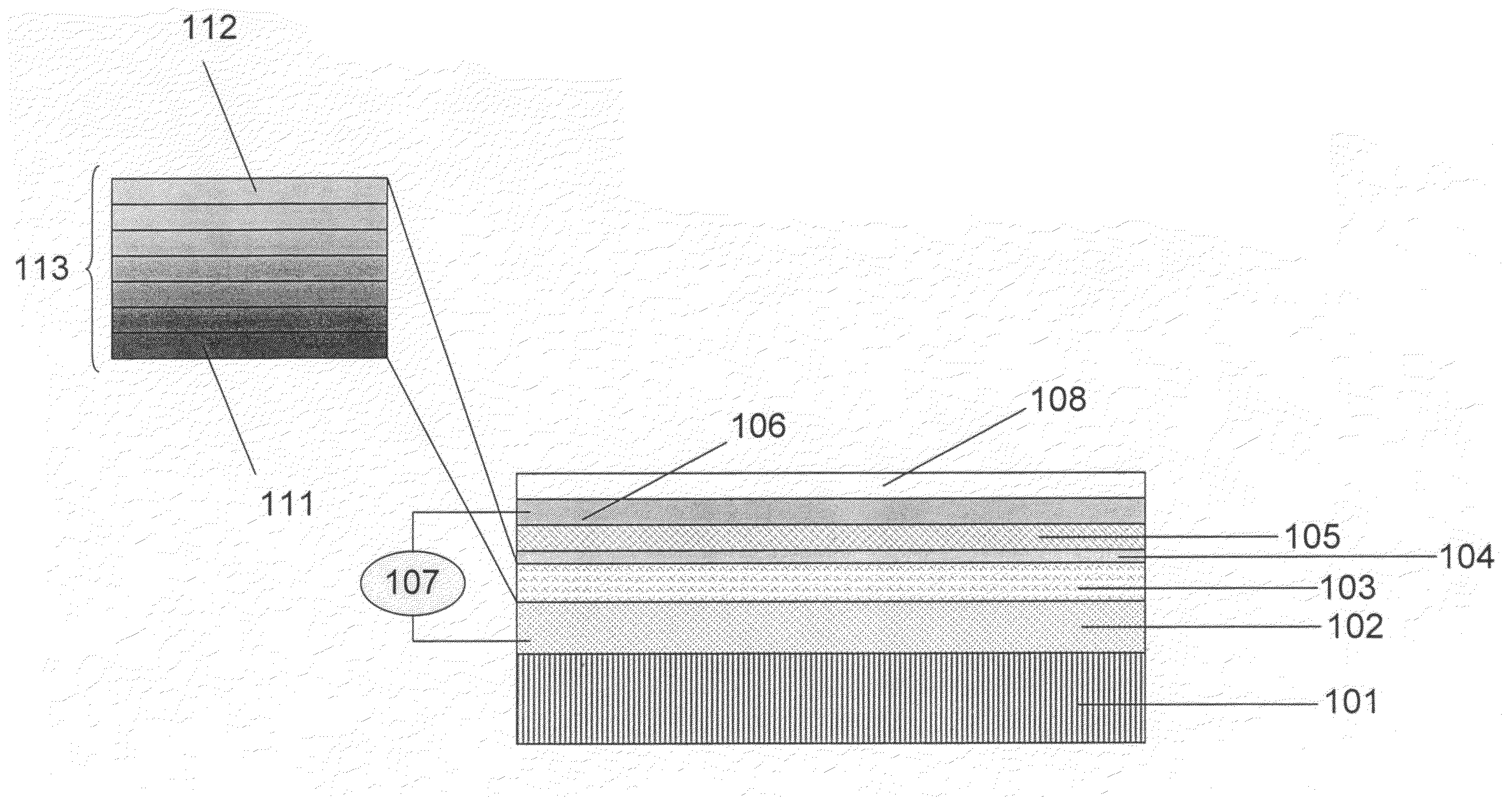
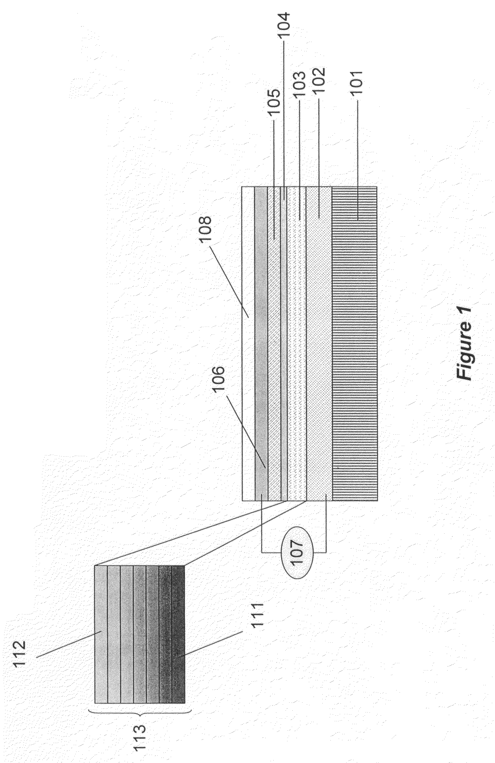
[0035]Copper (19.278 g), indium (80.36 g), and gallium (20.916 g) were mixed in a graphite crucible under argon at 800° C., stirred to mix, and allowed to cool. The resulting ingot was crushed into a powder. This powder was further reacted in a vapor condensation reactor at 1400° C. for one hour to yield copper-indium-gallium alloy nanoscale particles, with a final composition of Cu1In0.7Ga0.3. A portion of the resulting nanoscale alloy (0.778 g) was placed in a graphite crucible and selenium (0.898 g) was added. The crucible was covered with a graphite lid, then placed in an oven and heated to 500° C. for 75 minutes in an inert atmosphere. The resulting CIGS photovoltaic absorber material was allowed to cool to room temperature.


PUM

PropertyMeasurementUnit
Temperatureaaaaaaaaaa
Thicknessaaaaaaaaaa
Thicknessaaaaaaaaaa

Abstract

A photo-absorbing layer for use in an electronic device; the layer including metal alloy nanoparticles copper, indium and/or gallium made preferably from a vapor condensation process or other suitable process, the layer also including elemental selenium and/or sulfur heated at temperatures sufficient to permit reaction between the nanoparticles and the selenium and/or sulfur to form a substantially fused layer. The reaction may result in the formation of a chalcopyrite material. The layer has been shown to be an efficient solar energy absorber for use in photovoltaic cells.

Description

BACKGROUND OF THE INVENTION[0001]1. Technical Field[0002]The inventions disclosed herein relate generally to the manufacture of materials for thin film photovoltaic cells. More specifically, the invention relates to an improved production process for making the active absorbing material containing metal alloy nanoparticles that allows for increased efficiency, reduced cost, and reduced weight.[0003]2. Related Art[0004]A photovoltaic cell is a device that converts light energy directly into electricity. The high cost of polysilicon and resultant high cost of silicon solar cells has prevented widespread use of solar energy. Recent advances in low cost, high efficiency, thin film polycrystalline solar cells based on copper-indium-gallium-selenium-sulfide (CIGS) absorption layers promises to make solar energy competitive with energy derived from fossil fuels. Although these materials have some of the highest efficiencies of all classes of solar cells, exceeding 15%, several steps in the...

Claims


Application Information

Patent Timeline
IPC IPC(8): H01L31/0216B22F3/10
CPCB22F3/1035B22F7/04H01L31/02168H01L31/0322Y10T428/12014H01L31/073H01L31/1832Y02E10/541Y02E10/543H01L31/048H01L31/0749Y02P70/50
Inventor CARPENTER, R. DOUGLASMALONEY, KEVIN D.
Owner BRICOLEUR PARTNERS LP
Why Eureka
Try Eureka