
Semiconductor structure and method of forming the structure

a semiconductor and semiconductor technology, applied in the direction of semiconductor devices, electrical equipment, transistors, etc., can solve the problem of limited depth of carbon implants

Inactive Publication Date: 2008-08-14
GLOBALFOUNDRIES INC
View PDF10 Cites 41 Cited by
  • Summary
  • Abstract
  • Description
  • Claims
  • Application Information

AI Technical Summary

Benefits of technology

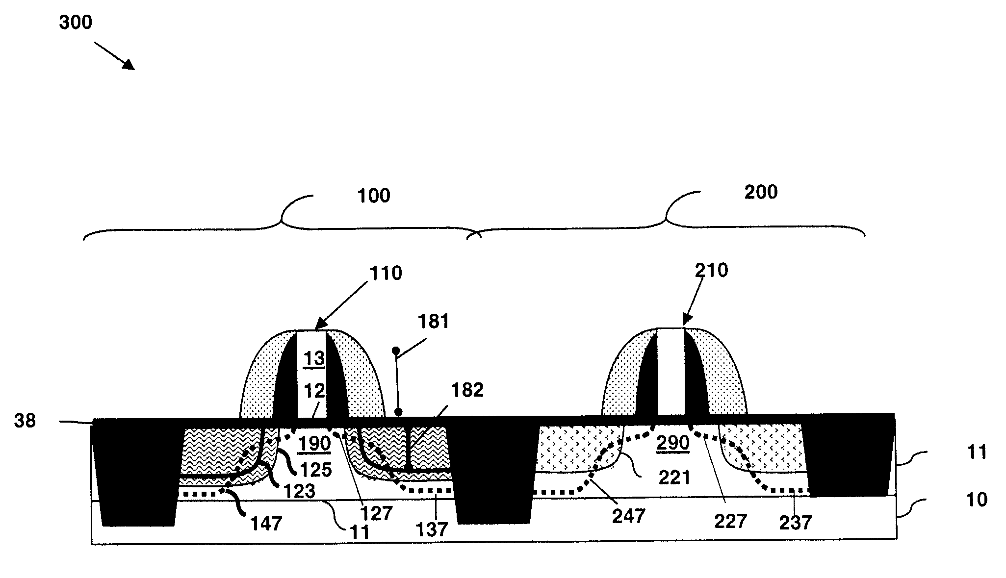
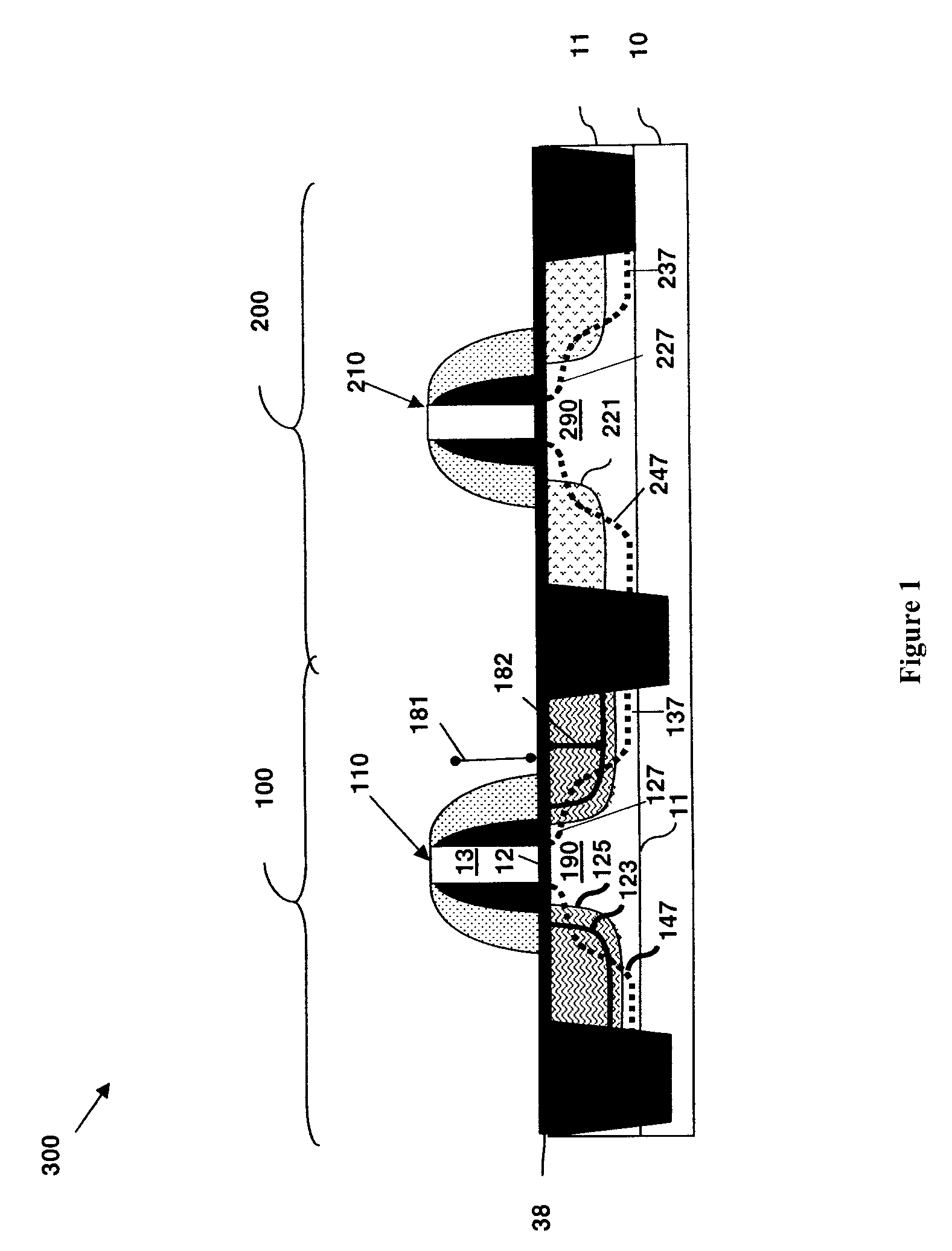
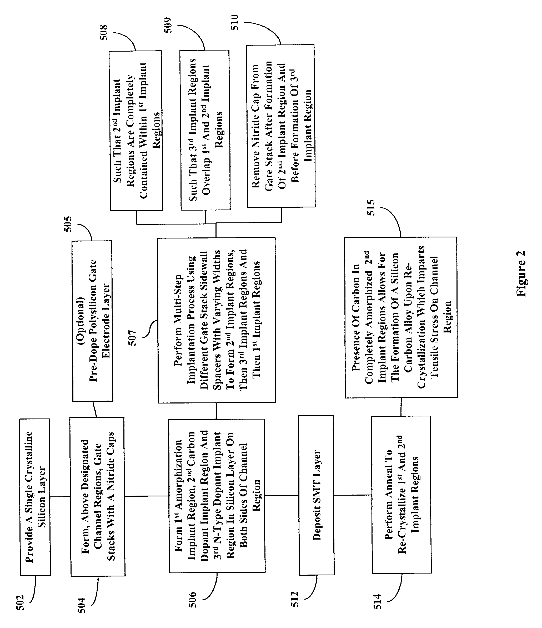
The patent describes an improved method for making n-type metal oxide semiconductor field effect transistors (n-FETs) and complementary metal oxide semiconductor devices (CMOS) that incorporate these n-FETs. The method includes a process for forming carbon implant regions on both sides of a channel region in a single crystalline silicon layer, followed by a nitride cap removal and n-type dopant deposition for deep source / drain and source / drain extension formation. The method also includes a process for forming a silicon carbon alloy in the second implant region to optimize tensile stress in the channel region. The semiconductor structure includes a semiconductor structure with improved carrier mobility in its channel region. The technical effects of the patent include improved performance and reliability of n-FETs and CMOS devices, as well as improved stress and strain optimization.

Problems solved by technology

Unfortunately, the deep carbon implant is limited because of the risk of simultaneously implanting carbon ions into the gate electrode and damaging the gate dielectric layer.

Method used


Image

  • Semiconductor structure and method of forming the structure
  • Semiconductor structure and method of forming the structure
  • Semiconductor structure and method of forming the structure

Examples


Embodiment Construction

[0047]The embodiments of the invention and the various features and advantageous details thereof are explained more fully with reference to the non-limiting embodiments that are illustrated in the accompanying drawings and detailed in the following description. It should be noted that the features illustrated in the drawings are not necessarily drawn to scale. Descriptions of well-known components and processing techniques are omitted so as to not unnecessarily obscure the embodiments of the invention. The examples used herein are intended merely to facilitate an understanding of ways in which the embodiments of the invention may be practiced and to further enable those of skill in the art to practice the embodiments of the invention. Accordingly, the examples should not be construed as limiting the scope of the embodiments of the invention.

[0048]As mentioned above, various stress memorization techniques are know for imparting the desired stress on n-FET and p-FET channel regions. F...


PUM

PropertyMeasurementUnit
stressaaaaaaaaaa
semiconductor structureaaaaaaaaaa
semiconductoraaaaaaaaaa

Abstract

Disclosed are embodiments of an n-FET structure with silicon carbon S / D regions completely contained inside amorphization regions and with a carbon-free gate electrode. Containing carbon within the amorphization regions, ensures that all of the carbon is substitutional following re-crystallization to maximize the tensile stress imparted on channel region. The gate stack is capped during carbon implantation so the risk of carbon entering the gate stack and degrading the conductivity of the gate polysilicon and / or damaging the gate oxide is essentially eliminated. Thus, the carbon implant regions can be formed deeper. Deeper S / D carbon implants which are completely amorphized and then re-crystallized provide greater tensile stress on the n-FET channel region to further optimize electron mobility. Additionally, the gate electrode is uncapped during the n-type dopant process, so the n-type dopant dose in the gate electrode can be at least great as the dose in the S / D regions.

Description

BACKGROUND[0001]1. Field of the Invention[0002]The embodiments of the invention generally relate to metal oxide semiconductor field effect transistors (MOSFETS) and, more particularly, to a strained MOSFET with carbon-doped source / drain regions and a method of forming the MOSFET.[0003]2. Description of the Related Art[0004]Current flowing through an electric field in the channel region of a field effect transistors is proportional to the mobility of the carriers (e.g., electrons in n-type field effect transistors (n-FETs) and holes in p-type field effect transistors (p-FETs) in that channel region. Different strains on the channel region can effect carrier mobility and, thus, current flow. For example, compressive stress on a channel region of a p-FET can enhance hole mobility. Contrarily, tensile stress on a channel region of an n-FET can enhance electron mobility. Various stress engineering techniques are known for imparting the desired stress on n-FET and p-FET channel regions. F...

Claims


Application Information

Patent Timeline
Patent Type & Authority Applications(United States)
IPC IPC(8): H01L27/092H01L29/778H01L21/8238H01L21/336
CPCH01L21/26506H01L21/26513H01L21/28247H01L21/823807H01L21/823814H01L21/84H01L29/7848H01L29/1045H01L29/1083H01L29/165H01L29/6653H01L29/66636H01L29/7843H01L27/1203
Inventor LIU, YAOCHENGNARASIMHA, SHREESHONISHI, KATSUNORIRIM, KERN
Owner GLOBALFOUNDRIES INC
Learn More