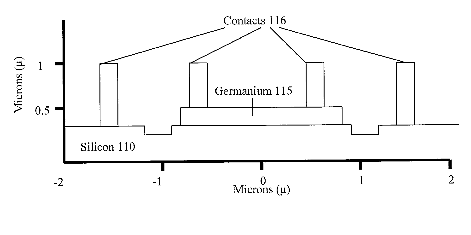
[0011]The current invention is an improved integrated waveguide photodiode. According to the current invention, optical losses associated with contacts to the
germanium layer of the silicon and germanium photodiode are reduced by positioning the contacts in proximity to predicted low
optical field regions at the top surface of the germanium layer. In some cases, the low
optical field regions may be predicted based on modeling and / or experimental data. In some examples according to the current invention, careful contact positioning may result in reduced optical scattering losses and / or optical absorption losses associated with the contacts. Reduced optical losses may result in more sensitive and / or less noisy devices. In some cases, design rules may be altered to incorporate the reduced optical losses and smaller and / or more compact devices may be designed and / or manufactured.
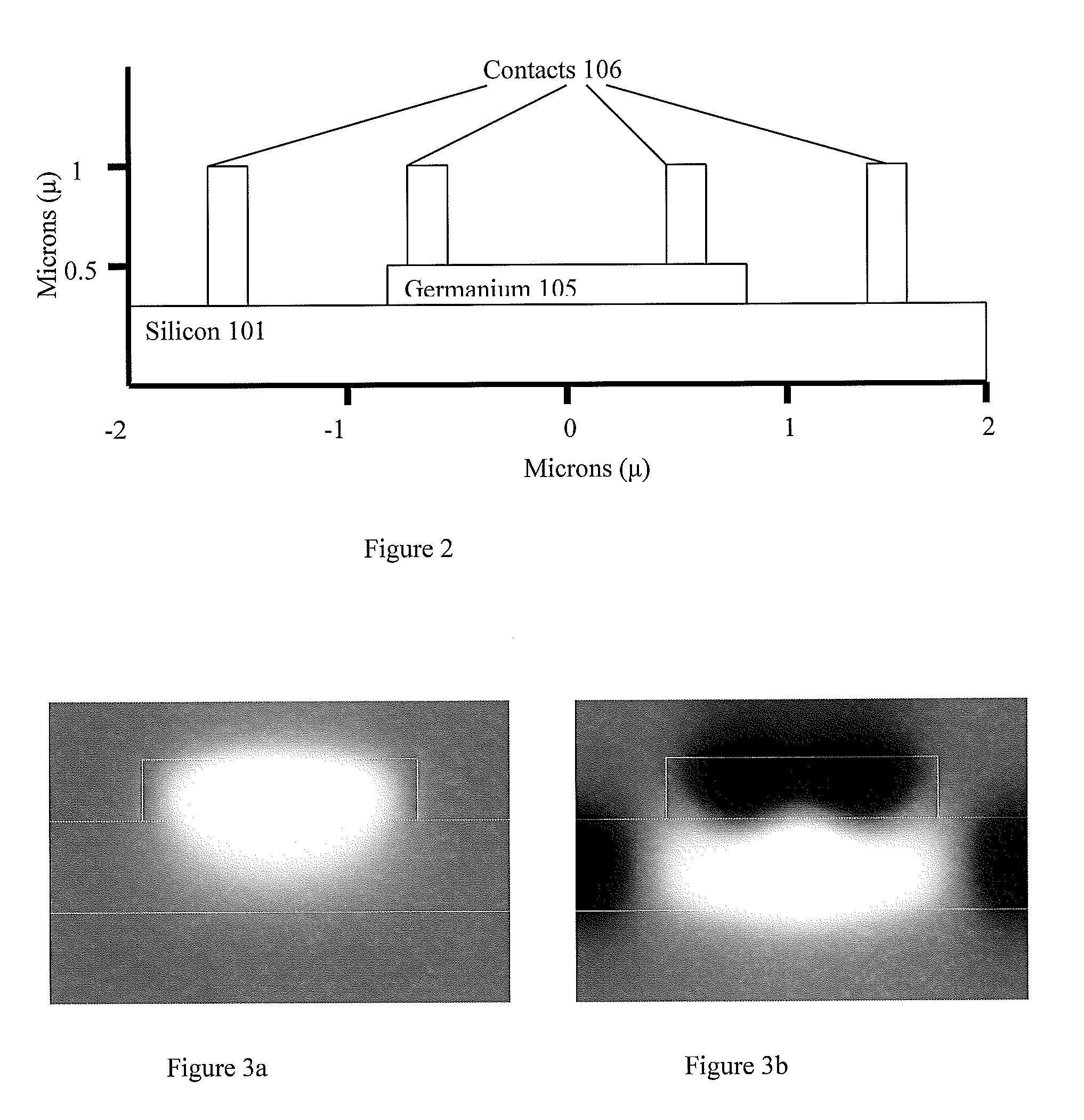
[0012]According to the current invention, lateral confinement of light in the silicon layer of the silicon and germanium photodiode may be improved and optical losses may be reduced by establishing side trenches along at least some portion of the length of the photodiode. In depth, the side trenches extend at least partially into the silicon layer; in length, the side trenches are adjacent to the germanium
detector. In some cases, the trenches may be substantially parallel to the edge of the germanium layer in the photodiode. In some cases, the trenches may vary in width. For example, in some examples according to the current invention, trenches may be used in conjunction with a tapered germanium layer. In some cases, the trench edges closest to the tapered germanium layer may be substantially parallel to the edge of the tapered germanium layer, whereas the far edges of the trenches may or may not be parallel to the tapered germanium layer. In some cases, the side trenches are filled with a
dielectric material such as, but not limited to, a silicon-oxi-
nitride (SiOxNy)
dielectric. Reduced optical losses in the silicon layer of the silicon and germanium photodiode portion of the integrated waveguide photodiode may enable more efficient
coupling of
optical power from the silicon layer to the germanium layer, possibly resulting in more sensitive and / or less noisy devices. In some cases, design rules may be altered to incorporate the reduced optical losses and smaller and / or more compact devices may be designed and / or manufactured.
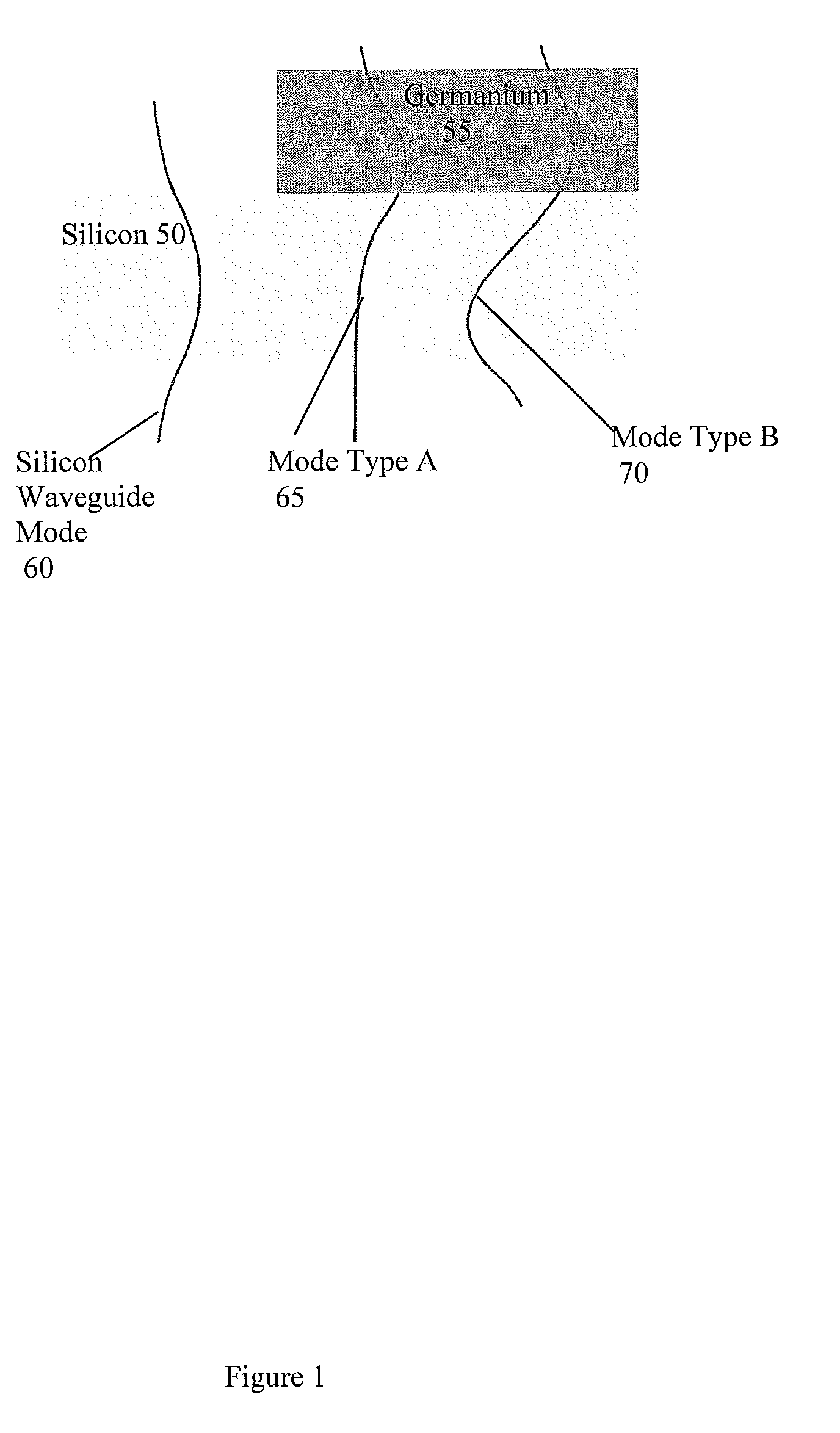
[0013]According to the current invention, a novel taper structure may be used to reduce optical losses when light is injected from the silicon layer to the germanium layer of a germanium on silicon integrated waveguide photodiode. For some examples of the current invention, the novel taper structure may be used to increase the overlap of the light with the germanium, to reduce the length of the waveguide photodiode while maintaining
responsivity, and / or to reduce the detrimental
impact of other loss mechanisms. According to the current invention, the geometry of a taper in the germanium layer of the silicon and germanium photodiode is selected at least in part based on the desirability of the expected operational
modes for a multimode
system. Preferred geometries would support
modes which anti-cross, converting unattractive modes into attractive modes. For example, an attractive mode might have a high overlap with the germanium layer, thereby improving the absorption in the germanium layer which may lead to attractive device characteristics. In some cases, different and / or additional considerations may be used to identify attractive modes such as, but not limited to, identifying modes which are “non-leaky” or have good lateral confinement.
Modal analysis based on proposed geometries,
coupling coefficients from the silicon waveguide into the integrated waveguide photodiode, and / or the effective indices of predicted dominant modes may be used, at least in part, to guide the design of a novel taper. According to the current invention,
modal analysis may be used to identify an appropriate initial taper width, an intermediate taper width, a taper grade, a final taper width and / or a taper length. In some cases, other considerations may be used to identify appropriate taper parameters such as, but not limited to, device
capacitance considerations and / or manufacturing constraints related to germanium thickness control, minimum feature size and / or manufacturable feature shape.

