Plasma processing apparatus

a processing apparatus and technology of plasma, applied in the direction of plasma technique, electric discharge lamps, electric lighting sources, etc., can solve the problems of deteriorating the production yield of a semiconductor device or a display device, difficult to change the temperature of coolant the temperature cannot be raised and lowered at a high speed, so as to improve repeatability and reliability of processing performance, and achieve the effect of safety and reliability of operation performan

Active Publication Date: 2008-08-21
TOKYO ELECTRON LTD
View PDF2 Cites 48 Cited by
  • Summary
  • Abstract
  • Description
  • Claims
  • Application Information

AI Technical Summary

Benefits of technology

[0010]In view of the above, the present invention provides a plasma processing apparatus in which a heating element is provided in a high frequency electrode, capable of achieving safety and reliability of an operation performance of a heater power supply and also improving repeatability and reliability of a processing performance by minimizing a high frequency power loss occurring in a heater power feed line.
[0011]In accordance with the present invention, there is provided a plasma processing apparatus comprising a first high frequency power for outputting a first high frequency, electrically connected to a first electrode disposed inside a depressurizable processing chamber; a heater power supply electrically connected to a heating element provided in the first electrode via filter circuits for reducing noise of the first high frequency; air core primary inductors provided in primary stages of the filter circuits when seen from the heating element; and a grounded conductive case for surrounding or accommodating the primary inductors.
[0012]In the above configuration, the primary inductors of the filter circuits are air core coils. By greatly increasing the inductance of the air core coils, the high frequency power loss can be remarkably reduced compared to a coil having a small inductance or a coil having a magnetic core such as ferrite or the like. Further, by accommodating or arranging the air core coils in the conductive case having a ground potential while being separated from an inner wall of the case (by about 10 mm or more from experience), the stray capacitance of the air core coils can be reduced and, further, the RF power loss can be further decreased. Preferably, the case is made of a stainless steel having a high relative magnetic permeability.

Problems solved by technology

If the temperature of the substrate is not properly controlled, it is difficult to secure process uniformity on a surface of the substrate, thereby deteriorating a production yield of a semiconductor device or a display device.
However, the above method is disadvantageous in that it is difficult to change a temperature of the coolant at a high speed and, also, the temperature cannot be raised and lowered at a high speed due to poor responsiveness in temperature control.
Meanwhile, in case where a lower plate dual frequency application type in which a high frequency power supply is connected to a susceptor in view of plasma control and the above heater in which a heating element is provided in a susceptor in view of temperature control are used at the same time, if a part of a high frequency applied to the susceptor enters a heater power supply via a heater power feed line, an operation or a performance of the heater power supply may deteriorate.
Especially, the heater power supply capable of high-speed control performs an ON / OFF control or a switching control with high sensitivity by using a semiconductor switching device such as an SSR (solid state relay) or the like, so that misoperation may easily occur by high frequency noise.
However, the inventors of the present invention have found, during the development and the evaluation of a plasma processing apparatus using a heater in a susceptor together with applying a high frequency power to a lower plate, that the conventional filter circuit has a problem in processing performance.
Namely, they have found that the RF power loss in the conventional filter is so large that it cannot be neglected in the processing performance, in addition to a known fact that a predetermined correlation exists between a processing performance (e.g., an etching rate) and a loss of high frequency power applied from a high frequency power supply to a susceptor (i.e., the processing performance deteriorates as the RF power loss increases).
Moreover, the inventors of the present invention have found that the RF power loss in the filter circuit is not determined by the circuit design, and varies even between plasma apparatuses of a same configuration, thereby causing differences in the processing performance.

Method used


Image

  • Plasma processing apparatus
  • Plasma processing apparatus
  • Plasma processing apparatus

Examples


Embodiment Construction

[0035]The embodiments of the present invention will be described with reference to the accompanying drawings which form a part hereof.

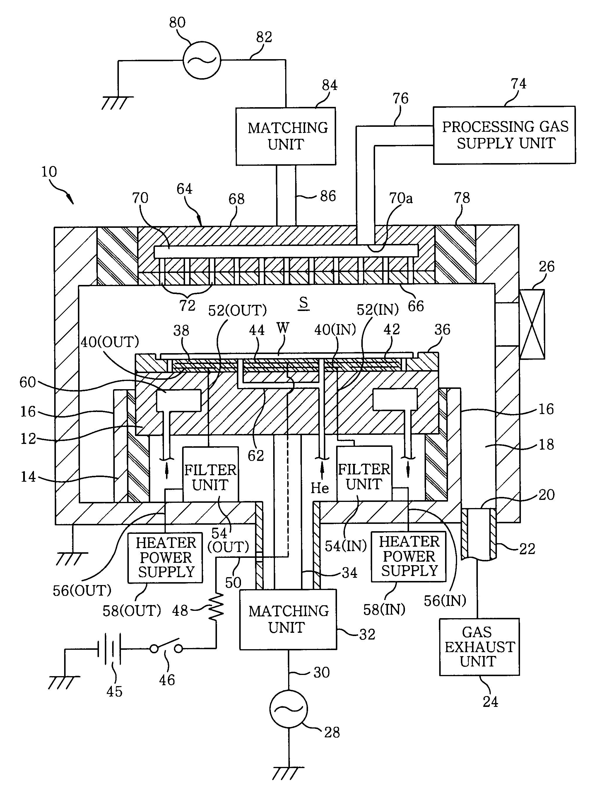
[0036]FIG. 1 shows a configuration of a plasma etching apparatus in accordance with an embodiment of the present invention. The plasma etching apparatus is configured as a capacitively coupled plasma etching apparatus having an upper-and-lower plate dual frequency application type, and has a cylindrical chamber (processing vessel) 10 made of a metal such as aluminum, stainless steel or the like. The chamber 10 is frame grounded.

[0037]A circular plate-shaped susceptor 12 for mounting thereon a target substrate, e.g., a semiconductor wafer W, is horizontally provided in the chamber 10 and serves as a lower electrode. The susceptor 12 is made of, e.g., aluminum, and is supported, without being grounded, by an insulating cylindrical supporting portion 14 vertically extended from a bottom of the chamber 10, the supporting portion 14 being made of, e.g., ce...


PUM

PropertyMeasurementUnit
stray capacitanceaaaaaaaaaa
inductanceaaaaaaaaaa
frequencyaaaaaaaaaa

Abstract

A plasma processing apparatus includes a first high frequency power for outputting a first high frequency, electrically connected to a first electrode disposed inside a depressurizable processing chamber; a heater power supply electrically connected to a heating element provided in the first electrode via filter circuits for reducing noise of the first high frequency. The plasma processing apparatus further includes air core primary inductors provided in primary stages of the filter circuits when seen from the heating element; and a grounded conductive case for surrounding or accommodating the primary inductors.

Description

FIELD OF THE INVENTION[0001]The present invention relates to a plasma processing apparatus in which a heating element is provided in a high frequency electrode inside a processing chamber capable of being depressurized; and, more particularly, to a plasma processing apparatus in which a filter circuit for blocking a high frequency is provided in a power feed line for supplying power to a heating element.BACKGROUND OF THE INVENTION[0002]When a semiconductor device or an FPD (flat panel display) is microprocessed by using a plasma, it is extremely crucial to control a temperature and a temperature distribution of a substrate and a plasma density distribution on a substrate to be processed (a semiconductor wafer, a glass substrate or the like). If the temperature of the substrate is not properly controlled, it is difficult to secure process uniformity on a surface of the substrate, thereby deteriorating a production yield of a semiconductor device or a display device.[0003]Generally, a...

Claims


Application Information

Patent Timeline
Patent Type & Authority Applications(United States)
IPC IPC(8): H05H1/00
CPCH01J37/32091H01L21/67098H01L21/67069H01J2237/2001
Inventor YAMAZAWA, YOHEI
Owner TOKYO ELECTRON LTD
Why Eureka
Try Eureka