Mask blank, method of manufacturing an exposure mask, and method of manufacturing an imprint template

a technology of mask and imprint, which is applied in the field of mask and exposure mask manufacturing methods, and the method of manufacturing an imprint template, can solve the problems of etching bias occurrence, resist reduction or disappearance, and difficulty in correction, and achieve the effect of high pattern accuracy

Active Publication Date: 2008-08-28
HOYA CORP
View PDF2 Cites 20 Cited by
  • Summary
  • Abstract
  • Description
  • Claims
  • Application Information

AI Technical Summary

Benefits of technology

[0013]In case where the dimension of the pattern becomes finer, restriction is imposed upon the thickness of the resist in addition to the problem of etching bias of the chromium film. If the thickness of the resist is greater than approximately three times the pattern width, there arise problems such as decrease in resolution during exposure of the resist and collapse of the resist pattern after the pattern is formed. In case where the chromium pattern is formed by dry etching using the chlorine-based gas containing oxygen, the resist is gradually eliminated by etching. If the thickness of the resist is reduced, the resist disappears before completion of formation of the chromium pattern and a part of the chromium pattern which should not be etched will be etched. In the dry etching using a chlorine-based gas containing oxygen, the resist of a thickness equal to or greater than the thickness of chromium is consumed. Furthermore, in order to remove nonuniformity in etching depth, additional etching or overetching of twice or more long is performed. During the additional etching, the thickness of the resist is reduced. Accordingly, in order to avoid disappearance of the resist in dry etching, the thickness of the chromium film is limited to about ⅓ of the thickness of the resist at maximum. For example, in case where the resist pattern having a width of 30 nm is formed, the thickness of the resist is 90 nm or less so as to avoid collapse of the pattern and the thickness of the chromium film is about 30 nm or less which is equal to or less than the pattern width so as to avoid disappearance of the resist after etching.
[0067]According to this invention, it is possible to provide a mask blank capable of forming a fine pattern with high pattern accuracy in manufacture of an exposure mask.

Problems solved by technology

When the pattern has a finer dimension, there arises a problem in forming, for example, a chromium pattern either by wet etching or dry etching.
On the other hand, the above-mentioned wet etching is disadvantageous in that the chromium pattern does not have vertical profiles in section, that the chromium film is etched in a horizontal direction in section to be varied in dimension with respect to the resist pattern (etching bias), and so on.
However, there arises a problem such as recession or disappearance of a resist.
Further, like in the wet etching, there is a problem of occurrence of the above-mentioned etching bias.
If the etching bias is different depending upon the width to be etched, it is difficult to perform correction, such as data bias, to preliminarily adjust a line width upon exposure.

Method used


Image

  • Mask blank, method of manufacturing an exposure mask, and method of manufacturing an imprint template
  • Mask blank, method of manufacturing an exposure mask, and method of manufacturing an imprint template
  • Mask blank, method of manufacturing an exposure mask, and method of manufacturing an imprint template

Examples


first embodiment

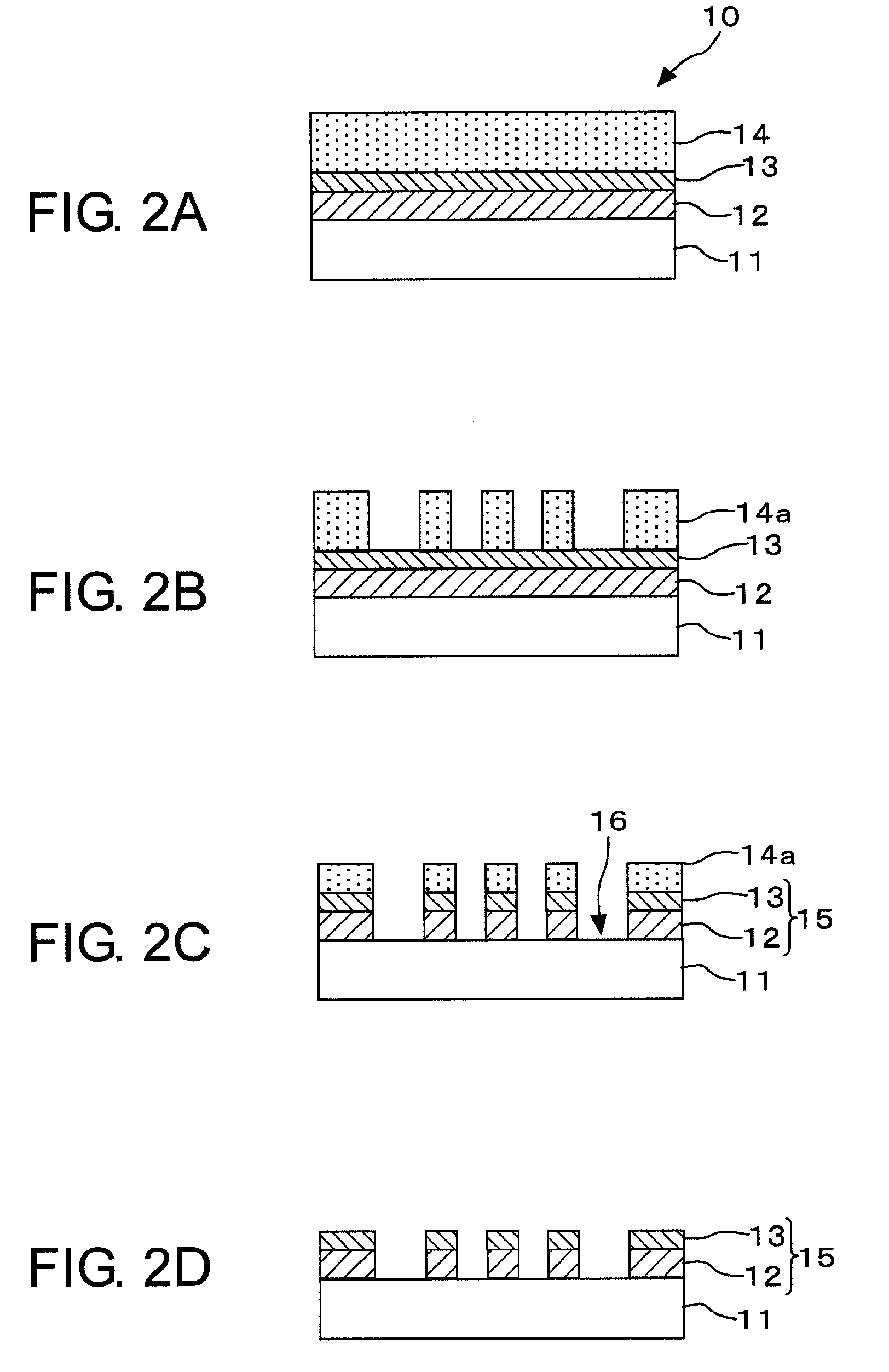
[0077]As a first embodiment, a binary mask for exposure by an ArF excimer laser will be described. FIGS. 2A to 2D show a manufacturing process of the binary mask according to the first embodiment.

[0078]A mask blank 10 used in this embodiment comprises a light-transmitting substrate 11 on which a laminate film composed of a light-shielding film 12 and a protective film 13 and serving as a thin film for forming a transfer pattern, and a resist film 14 are successively formed in this order. The mask blank 10 is prepared in the following manner.

[0079]As the light-transmitting substrate 11, a synthetic quartz substrate (having a size of 152 mm×152 mm and a thickness of 6.35 mm) was introduced into a sputtering apparatus. A target comprising an alloy of tantalum (Ta) and hafnium (Hf) (tantalum:hafnium=80:20 in atomic ratio) was sputtered by a xenon gas to deposit the light-shielding film 12 comprising a tantalum-hafnium alloy and having a thickness of 42 nm on the synthetic quartz substra...

second embodiment

[0084]As a second embodiment, a reflective mask for EUV exposure will be described. FIGS. 3A and 3B show a manufacturing process of the reflective mask according to the second embodiment.

[0085]A reflective mask blank 20 used in this embodiment comprises a substrate 21 on which a multilayer reflective film 22 for reflecting exposure light, a silicon film 23 formed on the multilayer reflective film 22, and a ruthenium-niobium alloy film 24, a laminate film which is composed of an absorber film 25 for absorbing the exposure light (for preventing reflection of the exposure light) and a protective film 26 and which serves as a thin film for forming a transfer pattern, and a resist film 27 are successively formed in this order. The ruthenium-niobium alloy film 24 serves to protect the multilayer reflective film 22 from the environment during patterning and pattern correction of the laminate film composed of the absorber film 25 and the protective film 26.

[0086]The reflective mask blank 20...

third embodiment

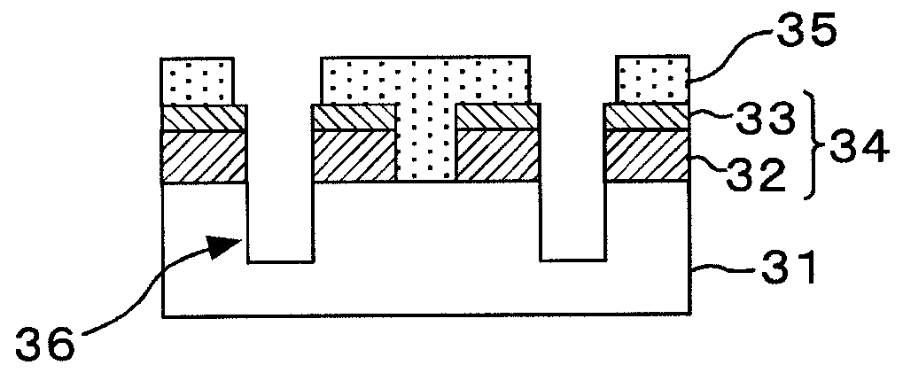
[0092]As a third embodiment, a phase shift mask for exposure by an ArF excimer laser will be described. FIGS. 4A and 4B show a manufacturing process of the phase shift mask according to the third embodiment.

[0093]A mask blank used in this embodiment comprises a light-transmitting substrate 31 on which a laminate film composed of a light-shielding film 32 and a protective film 33 and serving as a thin film for forming a transfer pattern, and a resist film are successively formed in this order.

[0094]The mask blank is prepared in the following manner like in the first embodiment. A target comprising an alloy of tantalum (Ta) and hafnium (Hf) (tantalum:hafnium=80:20 in atomic ratio) was sputtered by a xenon gas to deposit the light-shielding film 32 comprising a tantalum-hafnium alloy and having a thickness of 42 nm on a synthetic quartz substrate as the light-transmitting substrate 31. Thereafter, a chromium target was sputtered by a mixed gas of argon and oxygen to deposit the thin fi...


PUM

PropertyMeasurementUnit
widthaaaaaaaaaa
widthaaaaaaaaaa
thicknessaaaaaaaaaa

Abstract

A mask blank includes a substrate and a thin film formed thereon and used to form a pattern. The mask blank is adapted to be subjected to dry etching corresponding to a method of producing an exposure mask by patterning the thin film by dry etching using an etching gas substantially free from oxygen with a resist pattern formed on the thin film used as a mask. The thin film has a protective layer formed at least at its upper layer and containing 60 atomic % or more oxygen. For example, the dry etching is performed by the use of a chlorine-based gas substantially free from oxygen.

Description

[0001]This application is based upon and claims the benefit of priority from Japanese patent application No. 2007-49084, filed on Feb. 28, 2007, the disclosure of which is incorporated herein in its entirety by reference.BACKGROUND OF THE INVENTION[0002]This invention relates to a mask blank for use in producing an integrated circuit such as a semiconductor and an optical component having an optical function provided by a fine or microscopic pattern, a method of manufacturing an exposure mask, and a method of manufacturing an imprint template.[0003]Generally, in a manufacturing process of a semiconductor device or the like, a fine pattern is formed by the use of photolithography. In order to form the fine pattern, a plurality of substrates called photomasks are used. The photomask generally includes a light-transmitting glass substrate and a light-shielding fine pattern formed on the substrate and comprising a metal thin film or the like. In manufacture of the photomask, photolithog...

Claims


Application Information

Patent Timeline
Patent Type & Authority Applications(United States)
IPC IPC(8): G03F1/14G03F1/50G03F1/54G03F1/68
CPCB82Y10/00B82Y40/00G03F1/30G03F7/0002G03F1/54G03F1/58G03F1/80G03F1/32G03F1/50
Inventor NOZAWA, OSAMUKUREISHI, MITSUHIRO
Owner HOYA CORP
Why Eureka
Try Eureka