High etch resistant underlayer compositions for multilayer lithographic processes

a composition and lithography technology, applied in the field of bilayer lithography, can solve the problems of increasing the selectivity of resists to etch conditions for pattern transfer, increasing the requirements of sensitivity, transparency, aesthetics of images produced, and increasing the difficulty of achieving the effect of excellent etch resistance and film forming properties

Active Publication Date: 2008-08-28
FUJIFILM ELECTRONICS MATERIALS US
View PDF18 Cites 4 Cited by
  • Summary
  • Abstract
  • Description
  • Claims
  • Application Information

AI Technical Summary

Benefits of technology

[0022]The present disclosure is directed to thermally curable polymer compositions employing cycloolefin polymers with aromatic pendant groups to control optical absorbance and provide excellent etch resistance and film forming properties.

Problems solved by technology

As the patterns and wavelengths become finer, the material properties of the resists used for pattern delineation have become more and more demanding.
In particular, requirements of sensitivity, transparency, aesthetics of the image produced, and the selectivity of the resists to etch conditions for pattern transfer become more and more strenuous.
One problem is standing wave effects, which occur when monochromatic light is reflected off the surface of a reflective substrate during exposure.
These standing waves are variations of light intensity in the photoresist film dependent on photoresist film thickness caused by constructive and destructive interference of monochromatic light due to reflection.
This in turn reduces resolution and causes line width variations.
These line width changes are particularly troublesome for ever shrinking features.
For example, standing waves in a positive photoresist have a tendency to result in footing at the photoresist / substrate interface reducing the resolution of the photoresist.
However, this is difficult to do when the photoresist has to cover steps in the substrate topography.
Patterning over substrate topography can also cause localized reflections, which result in areas of the photoresist to be over or underexposed.
This reflective notching results in localized line width variations.
In addition, chemically amplified resist profiles and resolution may change due to substrate poisoning.
However, in order to decrease absorbance of the chemically amplified photoresists, aromatic groups, such as those in novolaks had to be removed, which in turn decreased the etch resistance.
A significant amount of photoresist is lost during the ARC etch process as the etch selectivity between resist and ARC is only about 1:1.
Even though the underlayer film attenuates standing waves and substrate poisoning, it poses other problems.
If there is intermixing between the resist when applied and the underlayer, the resolution and sensitivity of the imaging layer will be detrimentally affected.
If there is a large difference in the index of refraction between the chemically amplified resist and the underlayer film, light will reflect off the underlayer film which causes standing wave effects in the resist.
This results in low UL / IL interface reflectivity.
ARCs on the other hand need to be thin because of poor etch selectivity to the photoresist and in order to control substrate reflectivity they need to be highly absorbing.
Another problem with underlayers is that they are sometimes too absorbent because of incorporation of aromatic groups.
If the underlayer is too absorbent, the reflected light needed for alignment is too attenuated to be useful.
However, if the underlayer is not absorbent enough, standing waves may occur.
The problem with UV cross-linking underlayers is that they require long exposure times to form sufficient cross-links.
The long exposure times severely constrain throughput and add to the cost of producing integrated circuits.
The UV tools also do not provide uniform exposure so that some areas of the underlayer may be cross-linked more than other areas of the underlayer.
In addition, UV cross-linking exposure tools are very expensive and are not included in most resist coating tools because of expense and space limitations.
However, the problem with some of these underlayers is that they require high curing temperatures and long curing times before the resist for the imaging layer can be applied.
This can result in contamination of the equipment, which requires more frequent cleaning or replacement of equipment to avoid loss of product yield and other measures.
This results in increased costs and is undesirable.
However, this may be difficult to accomplish with underlayer films undergoing thermal crosslinking.
This makes it more difficult for the film to flow and planarize the substrate.
However, use of lower molecular weight polymers in the underlayer film can adversely impact the lithographic performance of the resist imaging process.
Conversely, acrylate-based polymers possess good optical transparency at 193 nm but suffer from poor etch resistance.
Solutions for these issues individually frequently adversely impact the performance in other areas.
However, it is not obvious how to employ these materials as an underlayer film and obtain all of the required properties of an underlayer film at the same time.

Method used


Image

  • High etch resistant underlayer compositions for multilayer lithographic processes
  • High etch resistant underlayer compositions for multilayer lithographic processes
  • High etch resistant underlayer compositions for multilayer lithographic processes

Examples


synthesis example 1-15

[0193]Cycloolefin polymers P-1 to P-15, P-19 and P-20 were prepared according to the general procedure for complete methanolysis of cycloolefin polymers. The composition of the cycloolefin polymers and analytical data are presented in Table 1.

synthesis example 16-18

[0194]Cycloolefin polymers P-16 to P-18 were prepared according to the general procedure for partial methanolysis of cycloolefin polymers. The composition of the cycloolefin polymers and analytical data are presented in Table 1.

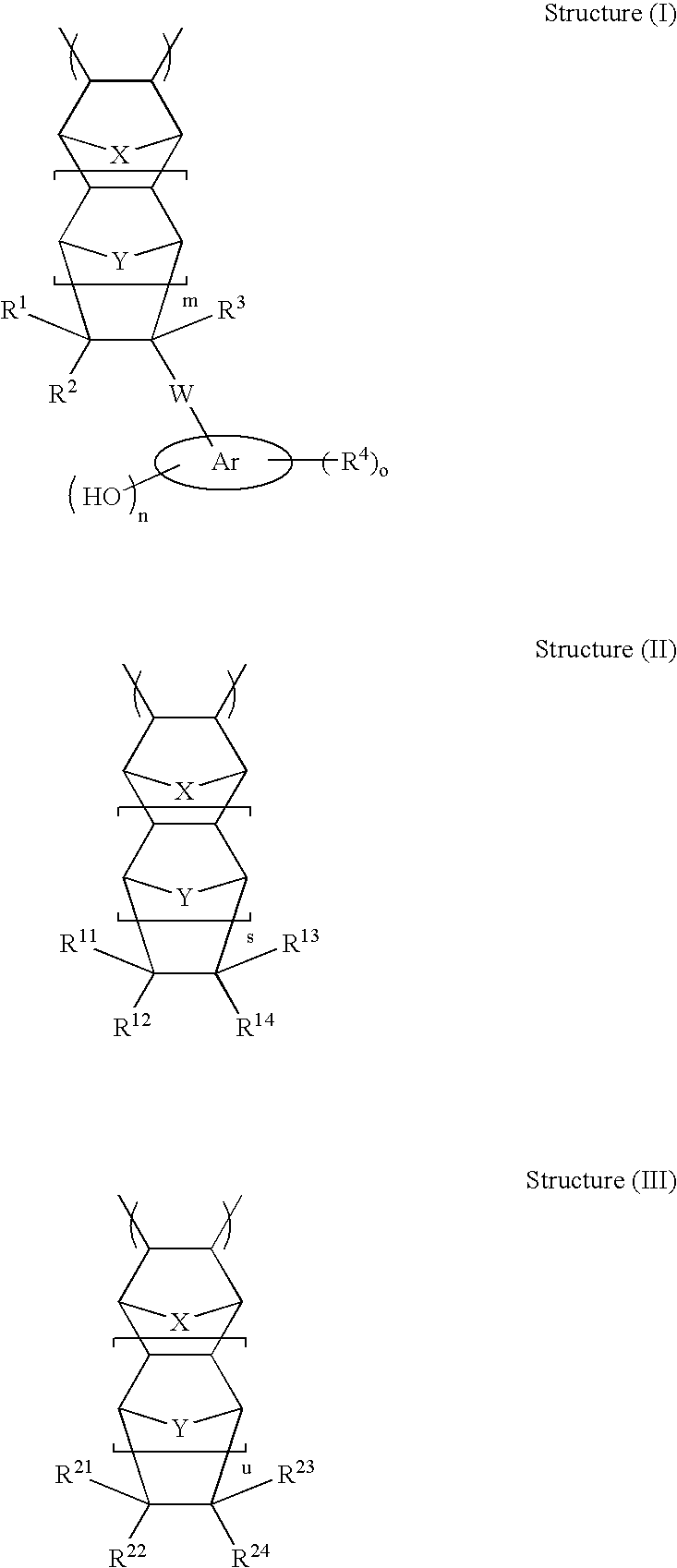
TABLE 1Composition and Analyticals of Cycloolefin polymerUnprotectedCycloolefinTGACycloolefinMolepolymer(5% WtpolymerCompositionRatio MWPDIloss)Tg (° C.)P-1NBPhOH-NBMeOH53 / 47102002.84350NDP-2NBPhOH-NBMeOH27 / 7380102.19——P-3NBPhOH-NBMeOH32 / 6859202.17——P-4NBPhOH-TDOH30 / 7033402.32——P-5NBPhOH-NBMeOH-30 / 28 / 4294802.15——HEANBP-6NBPhOH-NBMeOH-34 / 29 / 3797002.23——HEENBP-7NBPhOH-TDOH26 / 7491501.43350—P-8NBPhOH-TDOH26 / 74150001.48——P-9NBPhOH-NBMeOH47 / 5393202.64——P-10NBPhOH-NBMeOH46 / 5420601.96180P-11NBPhOH-TDOH26 / 7486001.49P-12NBPhOH-TDOH14 / 8685301.47——P-13NBPhOH / TDOH / TD25 / 15 / 60108602.0P-14NBPhOH / TDOH / TD25 / 35 / 4071301.6P-15NBPhOH / TDOH / TD25 / 55 / 2072501.6P-16NBPhOH-NBMeOAc27 / 7380102.19——P-17NBPhOH-NBMeOAc32 / 6859202.17——P-18NBPhOH-TDOAc30 / 7033402.32——P-19NBPhOH-TDOH25 / 7567401.41P-...

synthesis example 21-28

[0195]The general synthetic approach described in U.S. Pat. No. 6,232,417 (Example 1) is followed to prepare the base polymer before methanolysis. The reaction is allowed to run for 16 hours. The general methanolysis procedure is followed to remove the acetate groups. This yields polymers P-21 to P-28 (composition see Table 2)

TABLE 2Composition of Polymers P-21 to P28CycloolefineCompositionsMolePolymerStructure I TypeStructure II TypeRatioP-2130 / 70P-2230 / 70P-2330 / 70P-2430 / 70P-2530 / 70P-2630 / 70P-2730 / 70P-2830 / 70


PUM

PropertyMeasurementUnit
wavelengthaaaaaaaaaa

Abstract

An etch resistant thermally curable Underlayer for use in a multiplayer liyhographic process to produce a photolithographic bilayer coated substrate, the composition having:
    • (a) at least one cycloolefin polymer comprising at least one repeating unit of Structure (I), and at least one repeating unit of Structure (II), and optionally at least one repeating unit of Structure (III) with the proviso that neither Structure (I) nor Structure (II) nor Structure (III) contains acid sensitive groups.
    • b) at least one cross-linking agent selected from the group consisting of an amino or phenolic cross-linking agent;
    • c) a least one thermal acid generator (TAG);
    • d) at lest one solvent; and
    • e) optionally, at least one surfactant.

Description

RELATED APPLICATIONS[0001]This application claims priority from Provisional Patent Application No. 60 / 903,223 filed Feb. 23, 2007.FIELD OF THE DISCLOSURE[0002]The present disclosure relates to bilayer lithography used in semiconductor devices and more particularly to high etch resistant underlayer compositions for chemically amplified bilayer resist systems.BACKGROUND OF THE DISCLOSURE[0003]Microelectronic industries, as well as other related industries are constantly reducing the feature size for constructing microscopic structures. Effective lithographic techniques are essential in this quest and require constantly improved radiation sensitive materials (resists). In order to resolve smaller structures, the wavelength of the exposing light has been reduced into the deep UV regions of 248 nm, 193 nm and 157 nm in addition to exposure to EUV or x-ray radiation. As the patterns and wavelengths become finer, the material properties of the resists used for pattern delineation have beco...

Claims


Application Information

Patent Timeline
Patent Type & Authority Applications(United States)
IPC IPC(8): G03F7/004G03F7/00C08F12/24
CPCG03F7/091Y10S430/106G03F7/11
Inventor DE, BINOD B.MALIK, SANJAYSAKAMURI, RAJHONG, CHISUN
Owner FUJIFILM ELECTRONICS MATERIALS US
Why Eureka
Try Eureka