Release surfaces, particularly for use in nanoimprint lithography

a technology of nanoimprint lithography and release surface, which is applied in the direction of photomechanical equipment, instruments, manufacturing tools, etc., can solve the problems of high cost of x-ray lithography tools, economic impracticality of using these technologies for mass production of sub-50 nm structures, and inability to meet the requirements of lithography mass production, etc., to achieve enhanced resolution, low chemical reactivity, and more effective molding or microreplication processes

Inactive Publication Date: 2008-09-11
CHOU
View PDF6 Cites 22 Cited by
  • Summary
  • Abstract
  • Description
  • Claims
  • Application Information

AI Technical Summary

Benefits of technology

[0011]The present invention relates to a method for providing a surface with a treatment that can render the surface more effective in molding or microreplication processes. A molecular moiety having release properties towards other materials (e.g., fluorinated hydrocarbon chains or polysiloxanes) and low chemical reactivity to moldable polymers is bonded to a mold or microreplication surface. The release properties of the molecular moiety having release properties allows for the enhancement of resolution on the molded article since the molded material is released from the minute features of the mold on a molecular level. More common polymeric coated release surfaces can fill the openings or partially fill the openings of the mold. Merely smoother release surfaces expose the surface of the mold to abrasion and to reaction with the molding materials. The description of the coating as non-continuous may be described as follows. A continuous coating normally is one that forms a film on the surface with no direct route from one side of the film to the other side of the film. As there is no true film coating formed in the practice of the present invention, but rather individual molecules tend to be stacked up on the surface, there is no continuous coating, even though there may be uniform properties over the surface. On a molecular level, the surface would appear as a surface having one moiety at one end of a relatively linear molecule bonded to the surface. The relatively linear molecule extends away from the surface, with the release properties provided by the ‘tail’ of the molecule that extends away from the surface. The relative concentration of tails on the surface controls the hydrophilic / hydrophobic / polar / non-polar properties of the surface so that it will enable ready release of the material provided by the molding or microreplication process. The release portion of the adhered molecule will preferably have few reactive sites on the tail, particularly within the last one, two, three or four skeletal atoms in the relatively linear chain (e.g., with a hydrocarbon-based chain, the alpha, beta, gamma, and delta atoms in the chain). Such moieties to be avoided particularly would include free hydrogen containing groups (e.g., acid groups, carboxylic acid groups or salts, sulfonic acid groups or salts, amine groups, ethylenically unsaturated groups, and the like).
[0012]The present invention also relates to a method and apparatus for performing ultra-fine line lithography of the type used to produce integrated circuits and microdevices. A layer of thin film is deposited upon a surface of a substrate. A mold having its mold surface treated with the release materials of the present invention and at least one protruding feature and a recess is pressed into the thin film, therefore the thickness of the film under the protruding feature is thinner than the thickness of the film under the recess and a relief is formed in the thin film. The relief generally conforms to the shape of the feature on the mold. After the mold is removed from the film, the thin film is processed such that the thinner portion of the film in the relief is removed exposing the underlying substrate. Thus, the pattern in the mold is replicated in the thin film, completing the lithography. The patterns in the thin film will be, in subsequent processes, reproduced in the substrate or in another material that is added onto the substrate. The use of the release treatment on the mold surface enhances the resolution of the image and can protect the mold so that it can be used more often without showing wear on fine features in the mold.
[0013]The invention described here is based on a fundamentally different principle from conventional lithography. The process invention can eliminate many resolution limitations imposed in conventional lithography, such as wavelength limitation, backscattering of particles in the resist and substrate, and optical interference. It has been demonstrated the present invention can include a high throughput mass production lithography method for generating sub-25 nm features. Furthermore, the present invention has the ability to mass produce sub-10 nm features at a low cost. These capabilities of the present invention is unattainable with the prior art, and the use of the adherent release property coating improves the durability and the resolution of the process even further. The present process, however, has implications and utility for more macroscopic details in molding surfaces and would include features in the super-50 nm range, the super-100 nm range, and the super 200 nm range, as well as macroscopic dimensions in the visual range of features (e.g., 0.1 mm and greater).

Problems solved by technology

Numerous technologies have been developed to service these needs, but they all suffer serious drawbacks and none of them can mass produce sub-50 nm lithography at a low cost.
However, using these technologies for mass production of sub-50 nm structures seems economically impractical due to inherent low throughput in a serial processing tool.
But X-ray lithography tools are rather expensive and its ability for mass producing sub-50 nm structures is yet to be commercially demonstrated.
However, the practicality of such lithography as a manufacturing tool is hard to judge at this point.
However, no one has recognized the use of imprint technology to provide 25 nm structures with high aspect ratios.
Furthermore, the possibility of developing a lithographic method that combines imprint technology and other technologies to replace the conventional lithography used in semiconductor integrated circuit manufacturing has never been raised.

Method used


Image

  • Release surfaces, particularly for use in nanoimprint lithography
  • Release surfaces, particularly for use in nanoimprint lithography
  • Release surfaces, particularly for use in nanoimprint lithography

Examples


examples

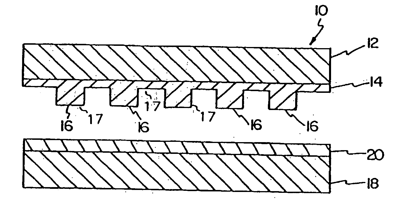
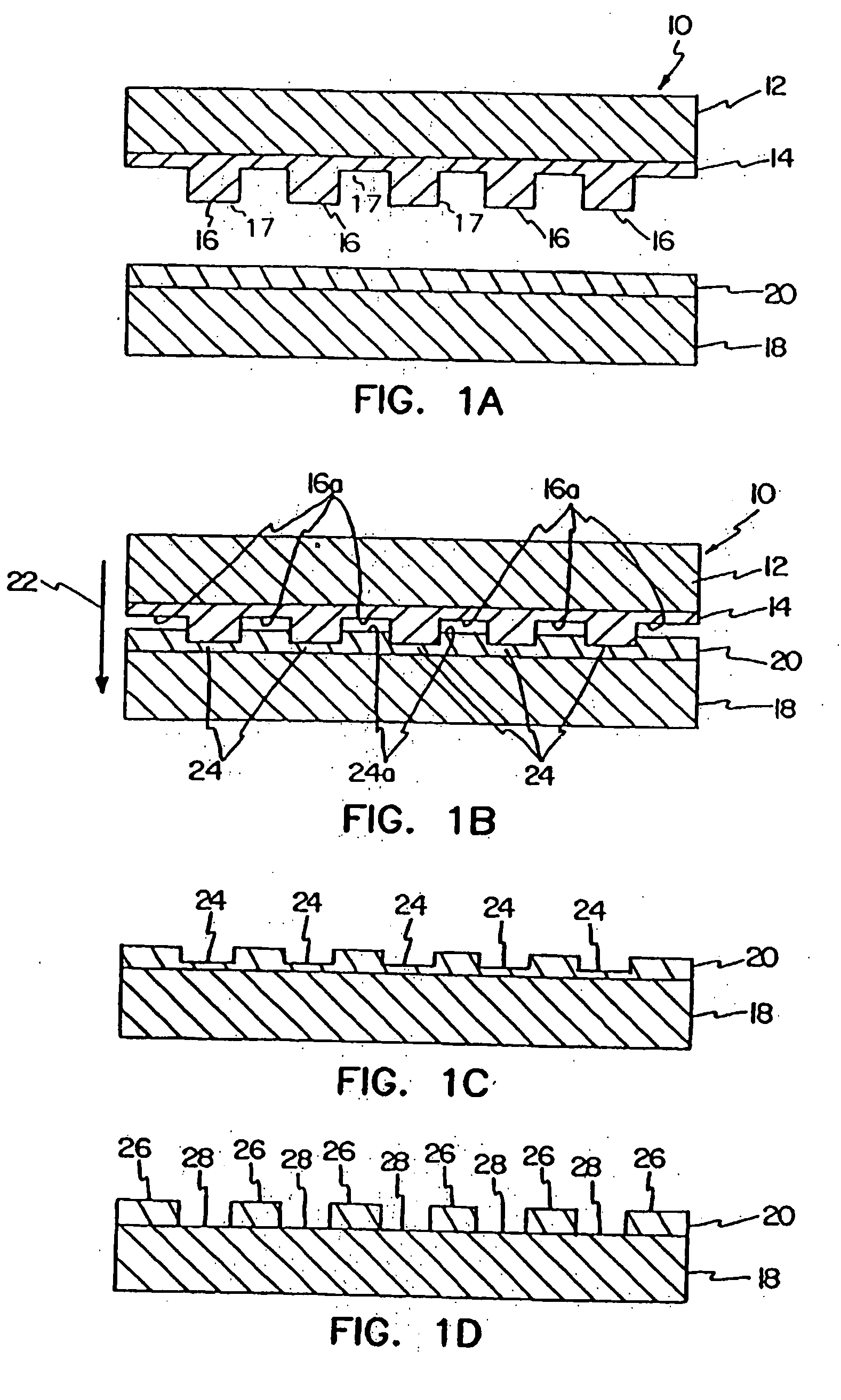
[0070]An example of a lithographic process according to the present invention forming a pattern in a film carried on a substrate would be practiced by the steps of depositing a film on a substrate to provide a mold having a protruding feature and a recess formed thereby, the feature and the recess having a shape forming a mold pattern. At least a portion of the surface, (in this case a surface of silica or silicon-nitride is preferred) such as the protruding feature(s), if not the entire surface (the protrusions and valleys between the protrusions) onto which the film is deposited, is coated with the release material comprises a material having the formula:

RELEASE-M(X)n-1—,  Formula I

RELEASE-M(X)n-m-1Qm  Formula II

or

RELEASE-M(OR)n-1—,  Formula III wherein

[0071]RELEASE is a molecular chain of from 4 to 20 atoms in length, preferably from 6 to 16 atoms in length, which molecule has either polar or nonpolar properties;

[0072]M is a metal or semimetal atom;

[0073]X is halogen or cyano, es...


PUM

PropertyMeasurementUnit
mold depthaaaaaaaaaa
depthaaaaaaaaaa

Abstract

The addition of thin coatings (less than and approaching monomolecular coatings) of persistent release materials comprising preferred compounds of the formula:
RELEASE-M(X)n-1
RELEASE-M(X)n-m-1Qm,
Or
RELEASE-M(OR)n-1—, wherein
    • RELEASE is a molecular chain of from 4 to 20 atoms in length, preferably from 6 to 16 atoms in length, which molecule has either polar or non-polar properties;
    • M is a metal atom, semiconductor atom, or semimetal atom;
    • X is a halogen or cyano, especially Cl, F, or Br;
    • Q is hydrogen or alkyl group;
    • M is the number Q represents
    • R is hydrogen, alkyl or phenyl, preferably hydrogen or alkyl of 1 to 4 carbon atoms; and
    • N is the valence −1 of M,
    • and n-m-1 is at least 1
provides good release properties. The coated substrates are particularly good for a lithographic method and apparatus for creating ultra-fine (sub-25 nm) patters in a thin film coated on a substrate is provided, in which a mold having at least one protruding feature is pressed into a thin film carried on a substrate. The protruding feature in the mold creates a recess of the thin film. The mold is removed from the film. The thin film then is processed such that the thin film in the recess is removed exposing the underlying substrate. Thus, the patterns in the mold is replaced in the thin film, completing the lithography. The patterns in the thin film will be, in subsequent process, reproduced in the substrate or in another material which is added onto the substrate.

Description

CROSS-REFERENCE TO RELATED APPLICATIONS[0001]This application is a continuation-in-part of U.S. patent application Ser. No. 10 / 244,276 filed Sep. 16, 2002, from which priority is claimed.[0002]The '276 application, in turn, is a continuation of U.S. patent application Ser. No. 10 / 046,594 filed by Stephen Chou on Oct. 29, 2001, which is a division of U.S. patent application Ser. No. 09 / 107,006 filed by Stephen Chou on Jun. 30, 1998 (now U.S. Pat. No. 6,309,580 issued Oct. 30, 2001) and which, in turn, is a continuation of U.S. patent application Ser. No. 08 / 558,809 filed by Stephen Chou on Nov. 15, 1995 (now U.S. Pat. No. 5,772,905 issued Jun. 30, 1998). The foregoing '276 application, '594 application, '006 application and '809 application, and each of the above identified patents are each incorporated herein by reference.STATEMENT REGARDING FEDERALLY SPONSORED RESEARCH[0003]Not Applicable.FIELD OF THE INVENTION[0004]The present invention relates to release surfaces, particularly re...

Claims


Application Information

Patent Timeline
Patent Type & Authority Applications(United States)
IPC IPC(8): B29C59/00
CPCB29C33/62B29C43/003B29C43/021B29C43/222B29C43/52G03F7/0002B29C2043/3211B29C2043/568B29C2059/023B82Y10/00B82Y40/00B29C2043/025
Inventor CHOU, STEPHEN Y.
Owner CHOU
Why Eureka
Try Eureka