Buffer layer for front electrode structure in photovoltaic device or the like

a photovoltaic device and buffer layer technology, applied in the direction of pv power plants, sustainable manufacturing/processing, final product manufacturing, etc., can solve the problems of unfavorable use, insufficient thickness of cds between cdte, and excessive surface roughness, etc., to achieve adequate work-function matching, good durability, and good durability

Inactive Publication Date: 2008-09-18
GUARDIAN GLASS LLC
View PDF99 Cites 79 Cited by
  • Summary
  • Abstract
  • Description
  • Claims
  • Application Information

AI Technical Summary

Benefits of technology

[0005]Certain example embodiments of this invention relate to a buffer layer provided in connection with a front electrode in a photovoltaic device or the like. In certain example embodiments, a front electrode structure includes a tin oxide based buffer layer that is provided between the front electrode and the semiconductor absorber film in a photovoltaic device. The tin oxide based buffer layer may be deposited via sputtering or the like, and may or may not be doped in certain example instances. In an example context of CdS / CdTe photovoltaic devices, the tin oxide based buffer layer is advantageous in that it (one or more of): (a) provides a good work-function match to the CdS / CdTe film and the front electrode; (b) provides good durability in that it is able to adequately withstand attacks of sulfur vapors at elevated temperatures during CdS / CdTe processing; (c) may be conductive; and / or (d) provides good mechanical durability.

Problems solved by technology

However, pyrolytically deposited fluorine-doped tin oxide TCOs have several drawbacks, such as considerable variation in sheet resistance across the lite and from batch to batch, and excessive surface roughness in certain instances.
The former drawback has a significant impact on voltage variation of completed photovoltaic devices, whereas the latter drawback can result in undesirably high numbers of pinholes in the TCO which in turn may require an increased thickness of CdS between CdTe and the TCO.

Method used


Image

  • Buffer layer for front electrode structure in photovoltaic device or the like
  • Buffer layer for front electrode structure in photovoltaic device or the like

Examples


Embodiment Construction

[0011]Referring now more particularly to the drawings in which like reference numerals indicate like parts throughout the several views.

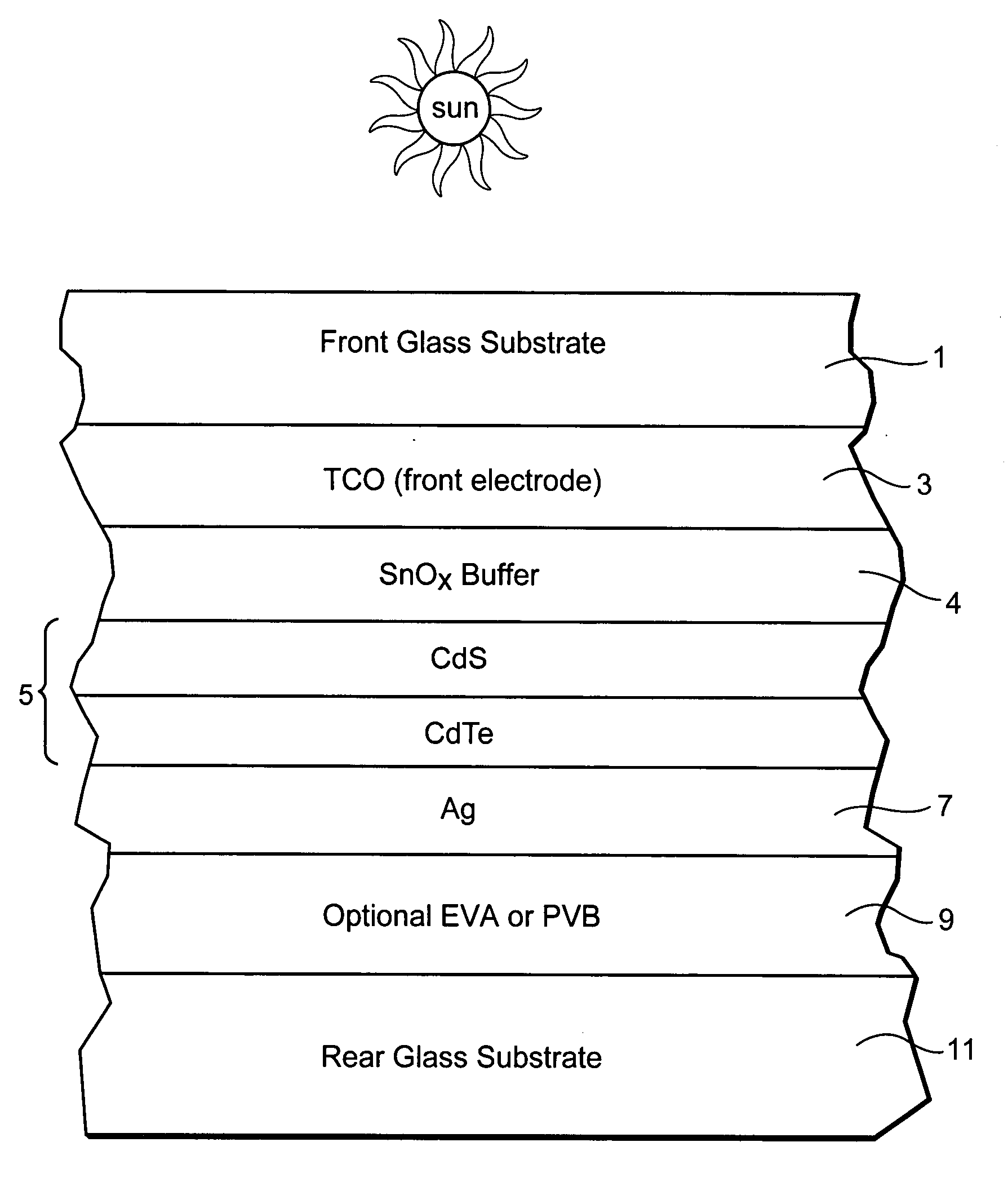
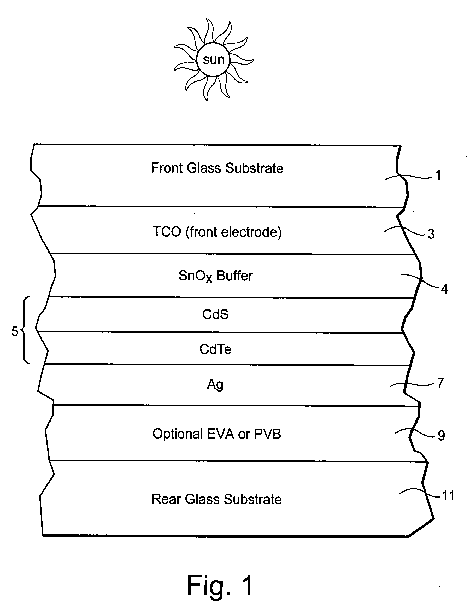
[0012]Photovoltaic devices such as solar cells convert solar radiation and other light into usable electrical energy. The energy conversion occurs typically as the result of the photovoltaic effect. Solar radiation (e.g., sunlight) impinging on a photovoltaic device and absorbed by an active region of semiconductor material (e.g., a semiconductor film including one or more semiconductor layers such as a-Si layers, or any other suitable semiconductor material such as CdS, CdTe and / or the like) generates electron-hole pairs in the active region. The electrons and holes may be separated by an electric field of a junction in the photovoltaic device. The separation of the electrons and holes by the junction results in the generation of an electric current and voltage. In certain example embodiments, the electrons flow toward the region of the semiconduct...


PUM

PropertyMeasurementUnit
work functionaaaaaaaaaa
thickaaaaaaaaaa
thicknessaaaaaaaaaa

Abstract

Certain example embodiments of this invention relate to an electrode structure (e.g., front electrode structure) for use in a photovoltaic device or the like. In certain example embodiments, a buffer layer (e.g., of or including tin oxide) is provided between the front electrode and the semiconductor absorber film in a photovoltaic device. The buffer layer may be deposited via sputtering, and may or may not be doped in certain example instances. In an example context of use in CdS/CdTe photovoltaic devices, the buffer layer is advantageous in that it (one or more of): (a) provides a good work-function match to a possible CdS/CdTe film and the front electrode; (b) provides good durability in that it is better able to withstand attacks of sulfur vapors at elevated temperatures during possible CdS/CdTe processing; (c) may be at least partially conductive; and/or (d) provides good mechanical durability.

Description

[0001]Certain example embodiments of this invention relate to a buffer layer provided in connection with a front electrode in a photovoltaic device or the like. In certain example embodiments, tin oxide based buffer layer is provided between the front electrode and the semiconductor absorber film in a photovoltaic device. The tin oxide based buffer layer may be deposited via sputtering, and may or may not be doped in certain example instances. In an example context of use in CdS / CdTe photovoltaic devices, the tin oxide based buffer layer is advantageous in that it (one or more of): (a) provides a good work-function match to the CdS / CdTe film and the front electrode; (b) provides good durability in that it is better able to withstand attacks of sulfur vapors at elevated temperatures during CdS / CdTe processing; (c) may be conductive; and / or (d) provides good mechanical durability.BACKGROUND AND SUMMARY OF EXAMPLE EMBODIMENTS OF INVENTION[0002]Photovoltaic devices are known in the art ...

Claims


Application Information

Patent Timeline
Patent Type & Authority Applications(United States)
IPC IPC(8): H01L31/042C23C14/00
CPCC03C17/347H01L31/056C03C17/36C03C17/3678C03C2217/734C03C2217/944C03C2217/948C23C16/407H01L31/022425H01L31/022466H01L31/03762H01L31/073H01L31/075H01L31/1884Y02E10/543C03C17/3476H01L31/022475H01L31/022483Y02P70/50
Inventor KRASNOV, ALEXEYLU, YIWEI
Owner GUARDIAN GLASS LLC
Why Eureka
Try Eureka