Method of magnetic tunneling junction pattern layout for magnetic random access memory

a random access memory and magnetic tunneling technology, applied in the direction of digital storage, instruments, semiconductor devices, etc., can solve the problems of affecting the performance of the magnetic tunneling junction, the difficulty of controlling the distance between the bit and the mtj from wafer to wafer, and the difficulty of the second approach in controlling the distance between the via layer and the mtj array, so as to achieve the effect of minimizing the delamination of the dielectric layer

Active Publication Date: 2008-09-18
TAIWAN SEMICON MFG CO LTD
View PDF4 Cites 29 Cited by
  • Summary
  • Abstract
  • Description
  • Claims
  • Application Information

AI Technical Summary

Benefits of technology

[0009]One objective of the present invention is to provide a MTJ pattern layout in a MRAM device that minimizes

Problems solved by technology

There is also a greater demand on reliability of the MRAM device since reduced MTJ sizes usually lead to a greater chance of device failure at contact points between adjacent metal layers and tend to cause delamination of the one or more interlayer dielectric (ILD) layers that separate the bit line and word line during CMP processing.
The second approach is not only costly but has difficulty in controlling distance between the BIT and MTJ fr

Method used


Image

  • Method of magnetic tunneling junction pattern layout for magnetic random access memory
  • Method of magnetic tunneling junction pattern layout for magnetic random access memory
  • Method of magnetic tunneling junction pattern layout for magnetic random access memory

Examples


Embodiment Construction

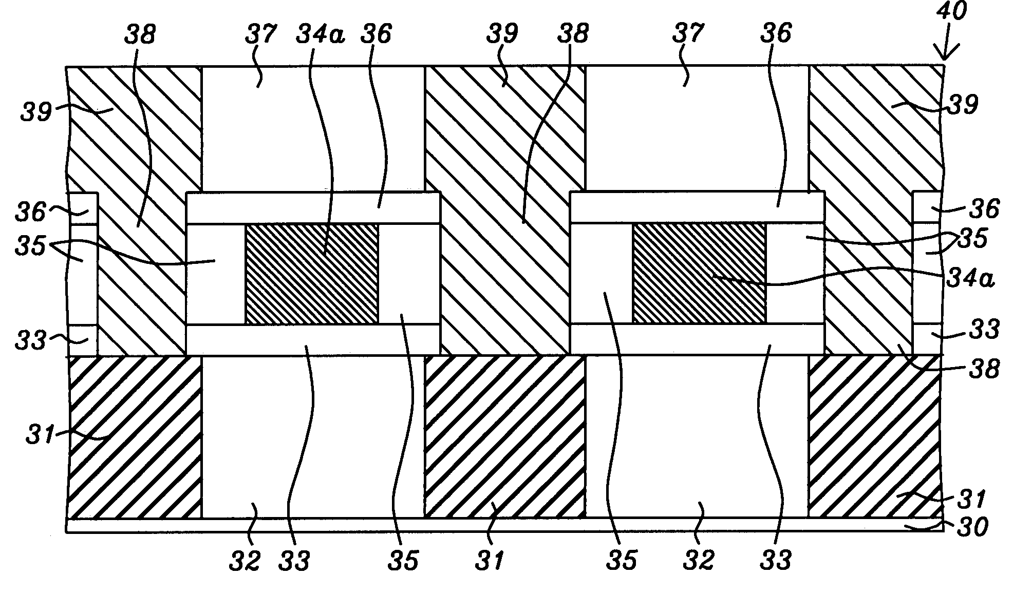
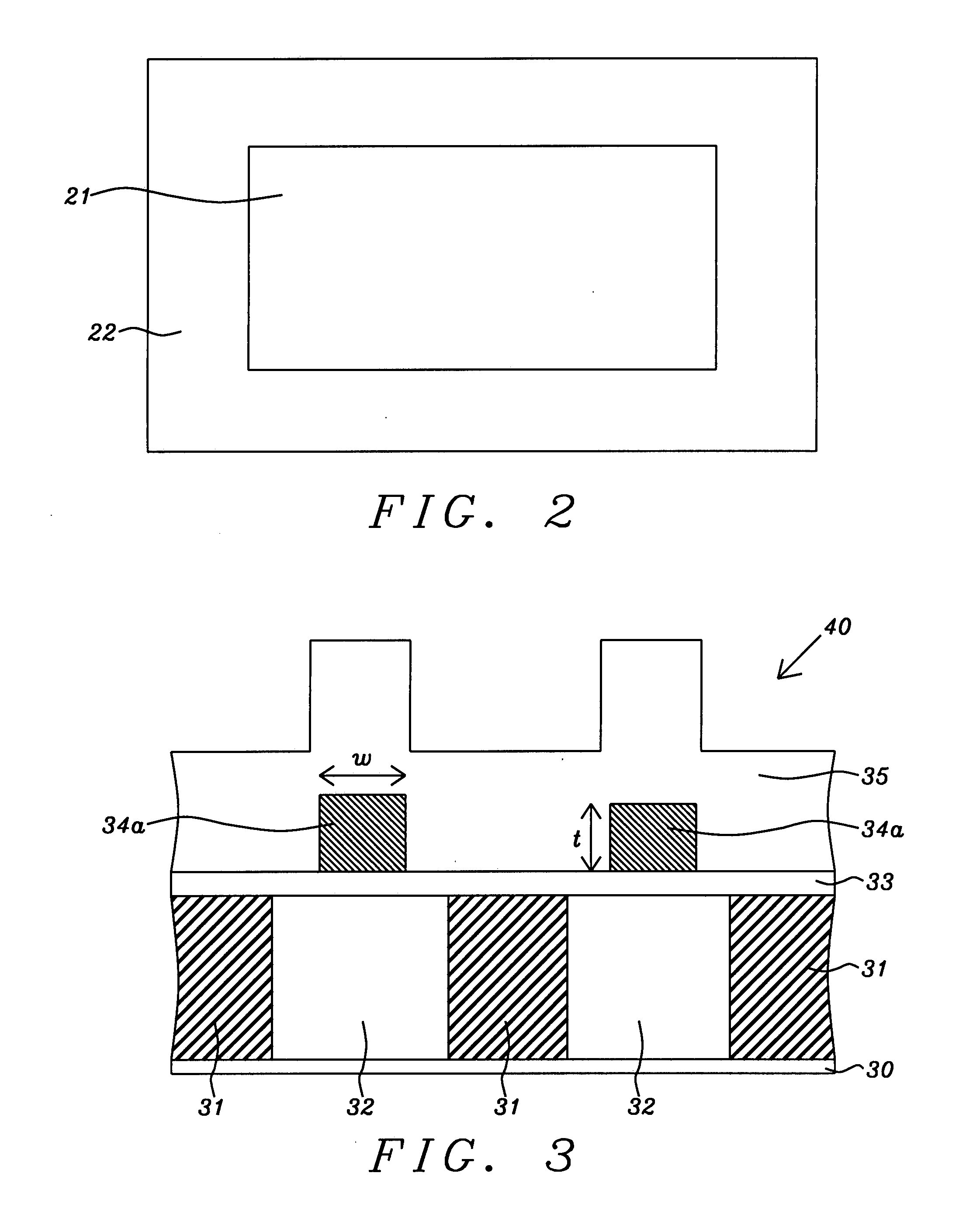
[0024]The present invention is a novel MTJ pattern layout that minimizes delamination of dielectric layers between a word line (WL) layer and a bit line (BIT) layer in a magnetic memory device, and minimizes dishing and protrusions following a CMP process that planarizes the BE / MTJ / hard mask stack and adjacent MTJ ILD layer. Although the exemplary embodiment depicts a MRAM device, the present invention may also apply to other magnetic memory devices known in the art that require a CMP process to stop on an array of MTJ devices. Drawings are provided by way of example and are not intended to limit the scope of the invention. For example, the number and position of MTJ devices or contact pads depicted in a particular design may not represent an actual layout used in manufacturing but are intended to show one possible layout that could be employed. The MTJ devices may have a top spin valve, bottom spin valve, or multi-layer spin valve configuration as understood by those skilled in the...


PUM


Abstract

An MTJ pattern layout for a memory device is disclosed that includes two CMP assist features outside active MTJ device blocks. A first plurality of dummy MTJ devices is located in two dummy bands formed around an active MTJ device block. The inner dummy band is separated from the outer dummy band by the MTJ ILD layer and has a MTJ device density essentially the same as the MTJ device block. The outer dummy band has a MTJ device density at least 10% greater than the inner dummy band. The inner dummy band serves to minimize CMP edge effect in the MTJ device block while the outer dummy band improves planarization. A second plurality of dummy MTJ devices is employed in contact pads outside the outer dummy band and is formed between a WL ILD layer and a BIT ILD layer thereby minimizing delamination of the MTJ ILD layer.

Description

FIELD OF THE INVENTION[0001]The invention relates to an improved magnetic tunneling junction (MTJ) pattern layout in a MRAM array and a method of forming the same that achieves superior chemical mechanical polishing (CMP) planarization and minimizes rework.BACKGROUND OF THE INVENTION[0002]Magnetic random access memory (MRAM) that incorporates a magnetic tunnel junction (MTJ) as a memory storage device is a strong candidate to provide a high density, fast (1-30 ns read / write speed), low power, and non-volatile solution for future memory applications. The architecture for MRAM devices is composed of an array of memory cells generally arranged in rows and columns. Each memory cell is comprised of a memory element (MTJ) that is in electrical communication with a transistor through an interconnect stack. The memory elements are programmed by a magnetic field created from pulse current carrying conductors such as copper lines. Typically, two arrays of current carrying conductors that may ...

Claims


Application Information

Patent Timeline
IPC IPC(8): G11C11/00
CPCH01L43/12H01L27/222Y10S977/935H10B61/00H10N50/01
Inventor ZHONG, TOMKO, TERRY KIN TINGTORNG, CHYU-JIUHKAN, WAI-MINGZHONG, ADAM
Owner TAIWAN SEMICON MFG CO LTD
Why Eureka
Try Eureka