Apparatus and method for manufacturing high purity polycrystalline silicon

a polycrystalline silicon and apparatus technology, applied in the field of apparatus and a manufacturing method of high purity polycrystalline silicon, can solve the problems of excessive current flow, low electrical resistance, and short supply of polycrystalline silicon, and achieve the effect of high purity

Inactive Publication Date: 2008-09-25
JNC CORP
View PDF2 Cites 9 Cited by
  • Summary
  • Abstract
  • Description
  • Claims
  • Application Information

AI Technical Summary

Benefits of technology

[0015]An apparatus for manufacturing a high purity polycrystalline silico

Problems solved by technology

However, as a polycrystalline silicon that is a raw material of a silicon for a solar cell, it is a present situation that a scrap such as a crucible residue after a monocrystalline silicon for a semiconductor is removed and a cutting abatement debris of a monocrystalline silicon ingot is used.
Consequently, since a polycrystalline silicon to be used for a solar cell depends on a trend of the semiconductor industry in quality and quantity, the polycrystalline silicon is in short supply chronically as the situation now stands.
However, since the seed rod 50 is heated by a current conduction for the Siemens method, an excessive current must be flown to heat the seed rod as the rod shaped silicon is grown by an adhesion of a polycrystalline silicon and an electrical resistance is decreased by a gradual process.
Consequently, a growth limit exists due to a balance with an energy cost, and the running of a manufacturing facility is in a batch system, thereby deteriorating a production efficiency.
Moreover, an electric power consumption rate is large to a co

Method used


Image

  • Apparatus and method for manufacturing high purity polycrystalline silicon
  • Apparatus and method for manufacturing high purity polycrystalline silicon
  • Apparatus and method for manufacturing high purity polycrystalline silicon

Examples


Embodiment Construction

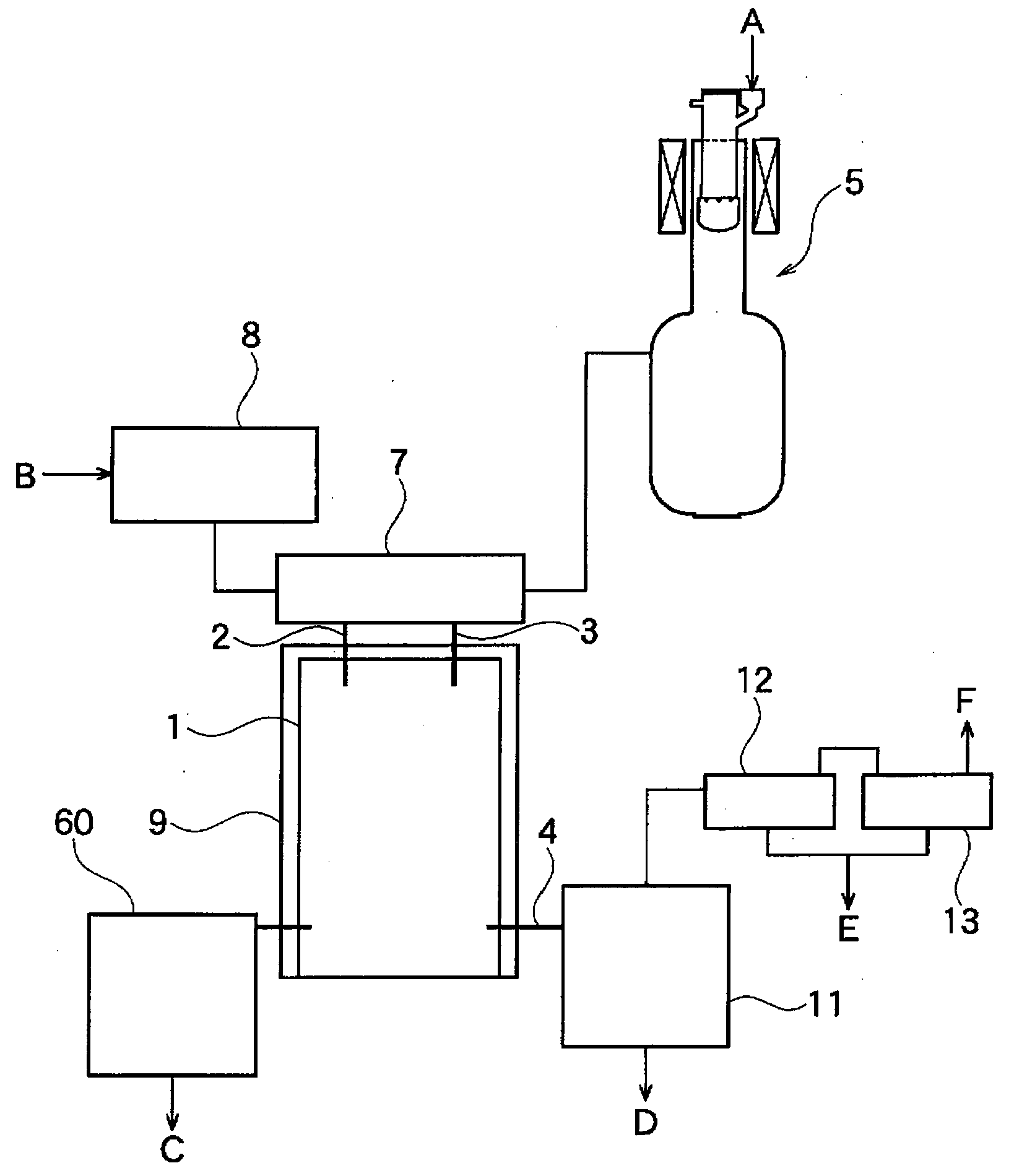
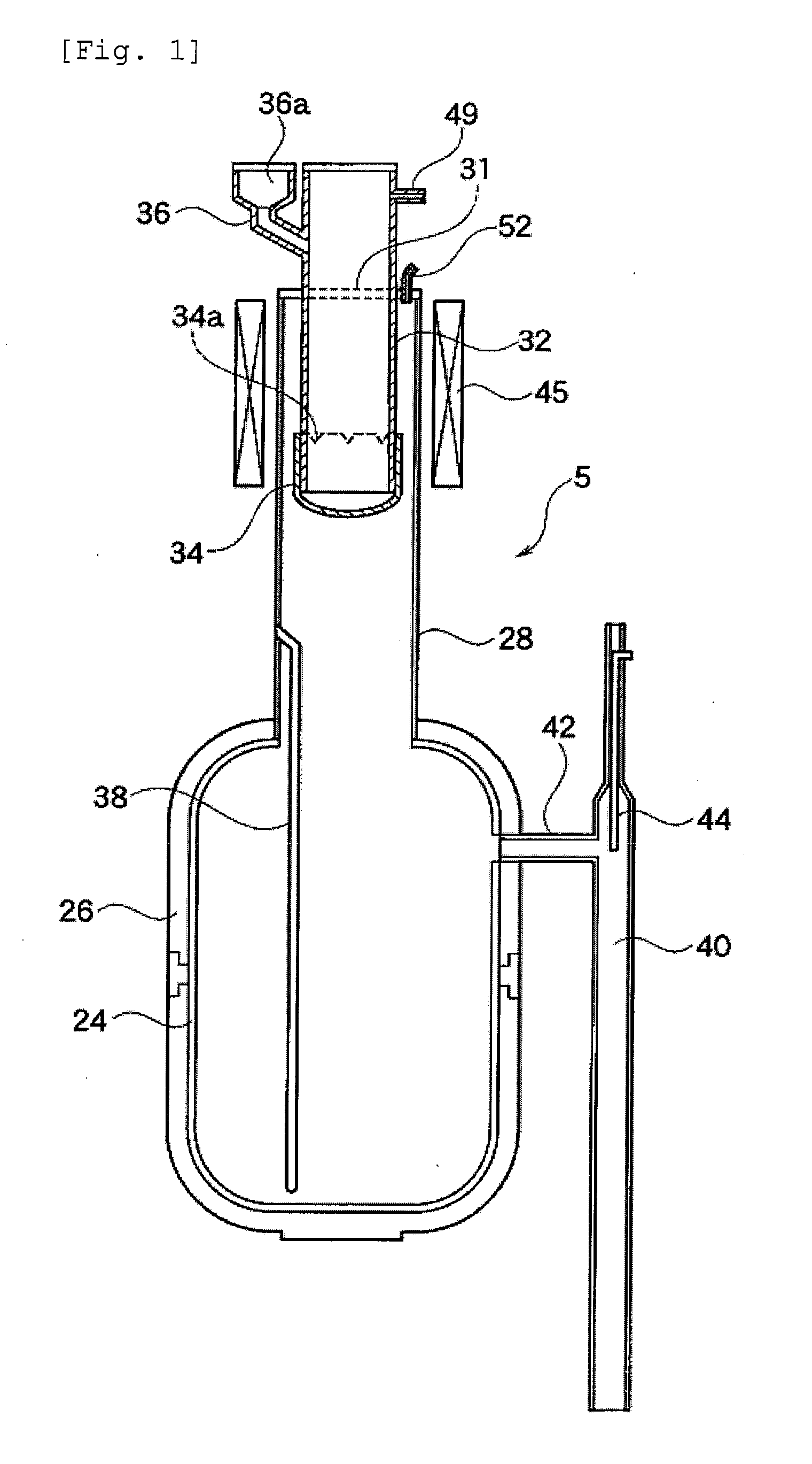
[0055]The invention includes:

[1] An apparatus for manufacturing a high purity polycrystalline silicon, comprising:

[0056]a vaporizer of silicon chloride;

[0057]a fusing evaporator of zinc;

[0058]a vertical reactor provided with a heating means on the peripheral face thereof;

[0059]a silicon chloride gas supply nozzle disposed to connect the vaporizer of silicon chloride and the vertical reactor and for supplying a silicon chloride gas supplied from the vaporizer of silicon chloride into the vertical reactor;

[0060]a zinc gas supply nozzle disposed to connect the fusing evaporator of zinc and the vertical reactor and for supplying a zinc gas supplied from the fusing evaporator of zinc into the vertical reactor; and

[0061]an exhaust gas vent pipe connected to the vertical reactor,

[0062]the fusing evaporator of zinc, further comprising:

[0063]a zinc evaporator;

[0064]a main vertical cylinder part connected to the upper part of the zinc evaporator;

[0065]a solid trapping pipe inserted into the m...


PUM


Abstract

An apparatus for manufacturing a high purity polycrystalline silicon is characterized by comprising: a vaporizer 8 of silicon chloride; a fusing evaporator 5 of zinc; a vertical reactor 1 provided with a heating means on the peripheral face thereof; a silicon chloride gas supply nozzle 2 disposed to connect the vaporizer 8 of silicon chloride and the vertical reactor 1 and for supplying a silicon chloride gas supplied from the vaporizer 8 of silicon chloride into the vertical reactor 1; a zinc gas supply nozzle 3 disposed to connect the fusing evaporator 5 of zinc and the vertical reactor 1 and for supplying a zinc gas supplied from the fusing evaporator 5 of zinc into the vertical reactor 1; and an exhaust gas vent pipe 4 connected to the vertical reactor 1, the fusing evaporator 5 of zinc, further comprising: a zinc evaporator 24; a main vertical cylinder part 28 connected to the upper part of the zinc evaporator 24; a solid trapping pipe 32 inserted into the main vertical cylinder part 28; a zinc introducing pipe 36 connected to the solid trapping pipe 32 at an angle; a seal pot 34 disposed to surround the lower end opening portion of the solid trapping pipe 32 and for configuring the bottom face of the solid trapping pipe 32; an induction heater 45 disposed on the peripheral face of the main vertical cylinder part 28 and capable of controlling a temperature; and a gas vent pipe 40 connected to the side wall of the zinc evaporator 24.

Description

CROSS-REFERENCE TO RELATED APPLICATION[0001]This application claims the priority benefit of Japan application serial no. 2007-071076, filed on Mar. 19, 2007. All disclosure of the Japan application is incorporated herein by reference.BACKGROUND OF THE INVENTION[0002]1. Field of the Invention[0003]The present invention relates to an apparatus and a method for manufacturing a high purity polycrystalline silicon.[0004]2. Description of the Related Art[0005]A polycrystalline silicon is used as a raw material of a monocrystalline silicon for a semiconductor or a raw material of a silicon for a solar cell. In recent years, according to the situation in which a diffusion of a solar cell is greatly expanded, a demand of a polycrystalline silicon have been increasing as a raw material of the solar cell in particular.[0006]However, as a polycrystalline silicon that is a raw material of a silicon for a solar cell, it is a present situation that a scrap such as a crucible residue after a monocr...

Claims


Application Information

Patent Timeline
IPC IPC(8): C01B33/021B01J19/00
CPCC01B33/033H01L21/205H01L21/22
Inventor NAMIKI, NOBUAKI
Owner JNC CORP
Why Eureka
Try Eureka