Fabrication of self-aligned gallium arsenide mosfets using damascene gate methods

Active Publication Date: 2008-10-02
MICRON TECH INC
View PDF4 Cites 42 Cited by
  • Summary
  • Abstract
  • Description
  • Claims
  • Application Information

AI Technical Summary

Benefits of technology

[0005]According to embodiments of the present invention, a process to fabricate self-aligned, inversion mode GaAs MOSFETS with excellent electric characteristics is presented. The process uses damascene gate methods enabling the deposition of the MOSFET gate stack after all the front-end-of-the-line (FEOL) hot processes are performed. In the damascene gate method, the α-Si/SiO2/HfO2/metal gate stack is deposited in a groove formed by removing a dummy gate. As technologies scale to smaller dimensions, the gate length of the GaAs MOSFET gets shorter, hence the α-Si/SiO2/HfO2 stack occupies an increasing fraction of the groove. In addition, the gate itself tends to be rounded at the bottom meaning that only the center of t

Problems solved by technology

In addition, the gate itself tends to be rounded at the bottom meaning that only the center of the gate has full control of the channel, and the pre

Method used


Image

  • Fabrication of self-aligned gallium arsenide mosfets using damascene gate methods
  • Fabrication of self-aligned gallium arsenide mosfets using damascene gate methods
  • Fabrication of self-aligned gallium arsenide mosfets using damascene gate methods

Examples


Example

[0010]In the following detailed description of the embodiments, reference is made to the accompanying drawings that form a part hereof, and in which are shown by way of illustration, and not by way of limitation, specific embodiments in which the invention may be practiced. It is to be understood that other embodiments may be utilized and that logical, mechanical and electrical changes may be made without departing from the spirit and scope of the present invention.

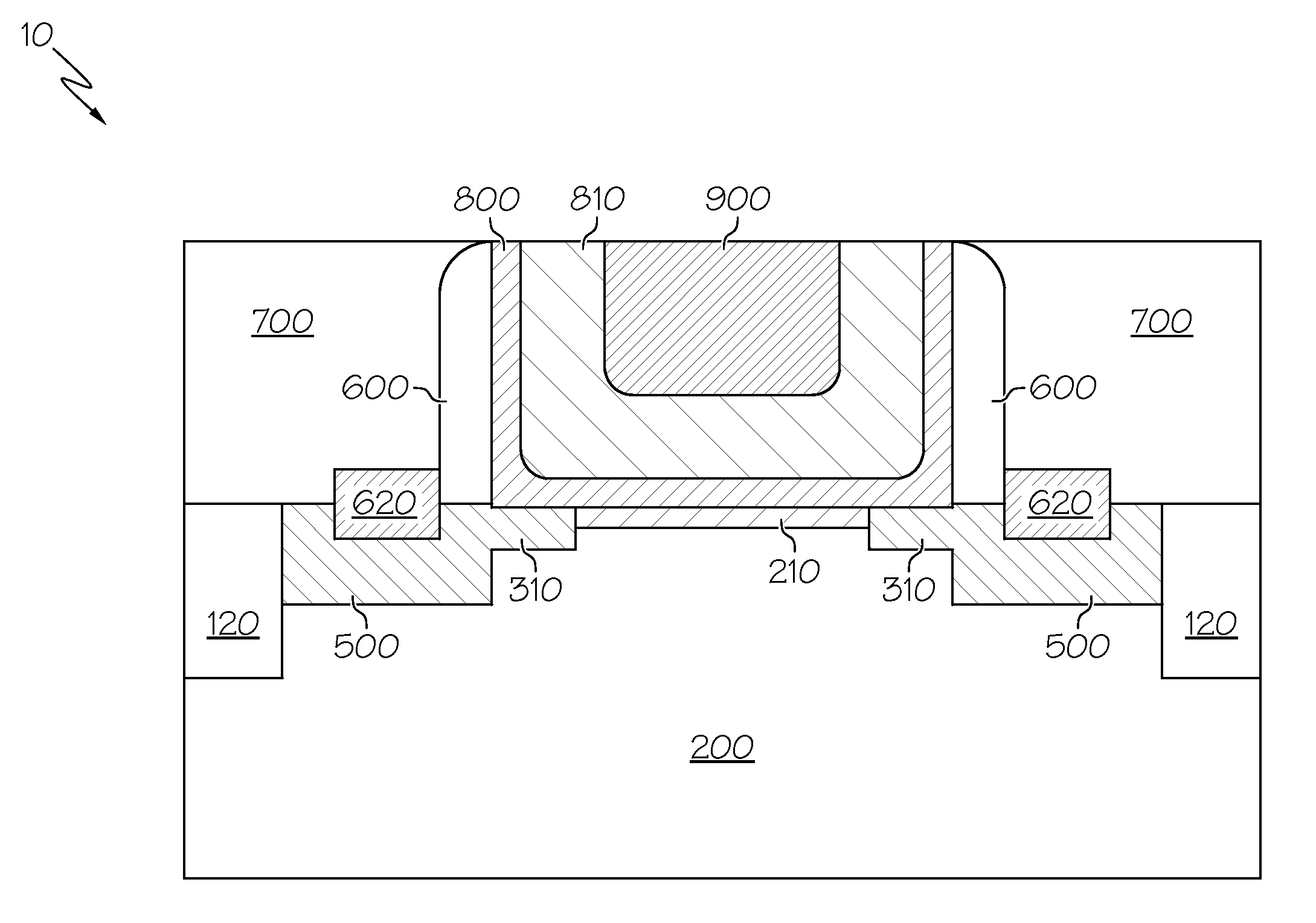
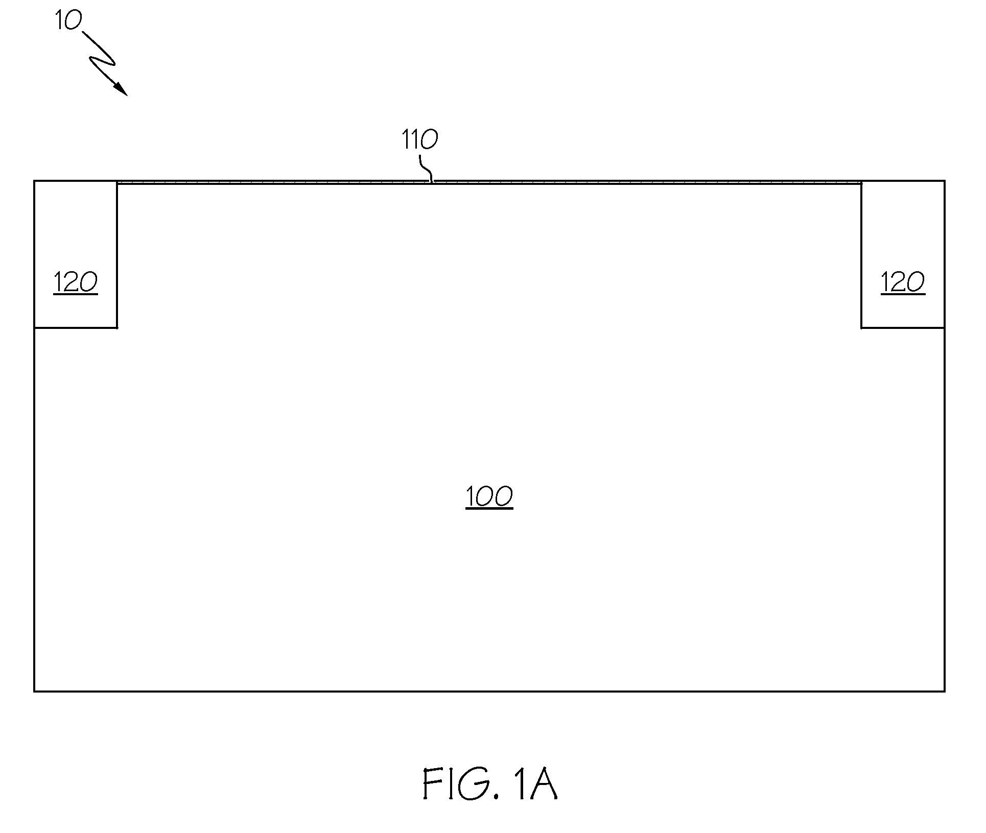
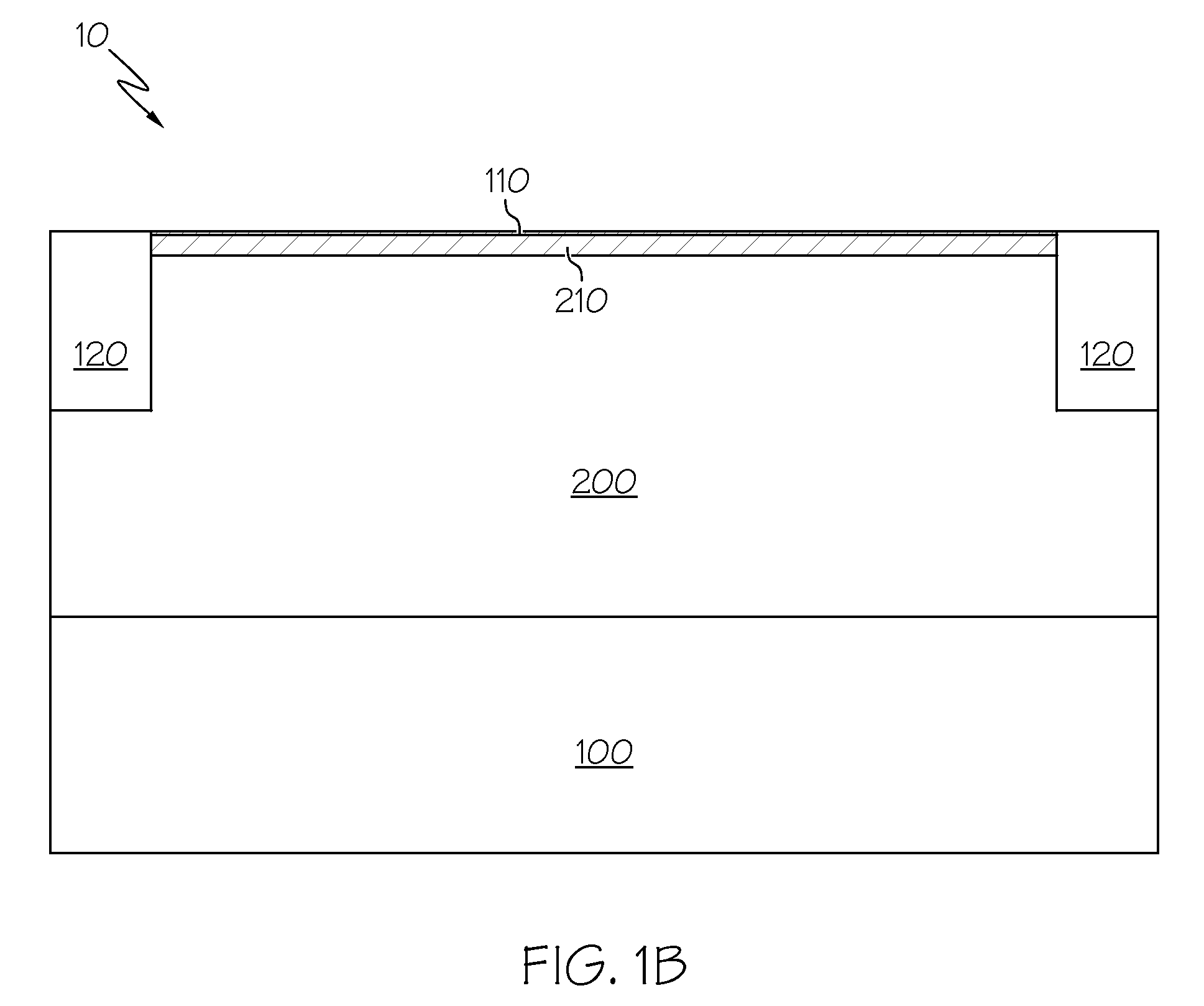
[0011]FIGS. 1a-1m illustrate the formation of a self-aligned GaAs MOSFET device 10 with high-k gate dielectrics using damascene gate methods in a stepwise fashion. Referring to FIG. 1a, a substrate 100 of bulk undoped orientated GaAs wafer is generally provided. A sacrificial oxide layer 110, comprising, for example, SiO2 or any other suitable sacrificial material, can be deposited over the substrate 100 using conventional deposition methods such as, for example, low pressure chemical vapor deposition (LPCVD). The thickn...


PUM


Abstract

A method for fabricating a gallium arsenide MOSFET device is presented. A dummy gate is formed over a gallium arsenide substrate. Source-drain extensions are implanted into the substrate adjacent the dummy gate. Dummy spacers are formed along dummy gate sidewalls and over a portion of the source-drain extensions. Source-drain regions are implanted. Insulating spacers are formed on dummy oxide spacer sidewalls. A conductive layer is formed over the source-drain regions. The conductive layer is annealed to form contacts to the source-drain regions. The dummy gate and the dummy oxide spacers are removed to form a gate opening. A passivation layer is in-situ deposited in the gate opening. The surface of the passivation layer is oxidized to create an oxide layer. A dielectric layer is ex-situ deposited over the oxide layer. A gate metal is deposited over the dielectric layer to form a gate stack in the gate opening.

Description

BACKGROUND OF THE INVENTION[0001]The present invention relates to fabricating self-aligned metal oxide semiconductor field effect transistors (MOSFETS), and more particularly, to fabricating self-aligned, inversion mode gallium arsenide MOSFETS with excellent electrical characteristics.[0002]The difficulty of increasing performance in sub-100 nm silicon (Si) complementary metal-oxide semiconductor (CMOS) technology has renewed interest in the use of Group III-V channel materials for advanced very large-scale integration (VLSI) CMOS. Gallium Arsenide (GaAs) is an attractive choice due to its relative maturity compared to other Group III-V compounds, its high electron mobility (˜6× compared to Si), and its lattice matching with germanium (Ge). The main barrier towards implementing enhancement—or depletion—mode GaAs MOSFETs for VLSI application is the difficulty of forming a high-quality gate insulator that passivates the interface states and prevents Fermi level pinning at the GaAs su...

Claims


Application Information

Patent Timeline
IPC IPC(8): H01L29/78H01L21/336
CPCH01L29/105H01L29/66522H01L29/6653H01L29/66545H01L29/66606
Inventor HANAFI, HUSSEIN I.
Owner MICRON TECH INC
Why Eureka
Try Eureka