Thin film capacitor
a thin film capacitor and capacitor technology, applied in the direction of capacitor details, electrical equipment, fixed capacitors, etc., can solve the problems of non-uniform side etching occurs inevitably, and the change in circumferential length is difficult to completely eliminate, so as to increase the mechanical strength of the protrusion, increase the pattern density, and increase the capacitance of the thin film capacitor
- Summary
- Abstract
- Description
- Claims
- Application Information
AI Technical Summary
Benefits of technology
Problems solved by technology
Method used
Image

Examples
configuration example 1
OF THIN FILM CAPACITOR
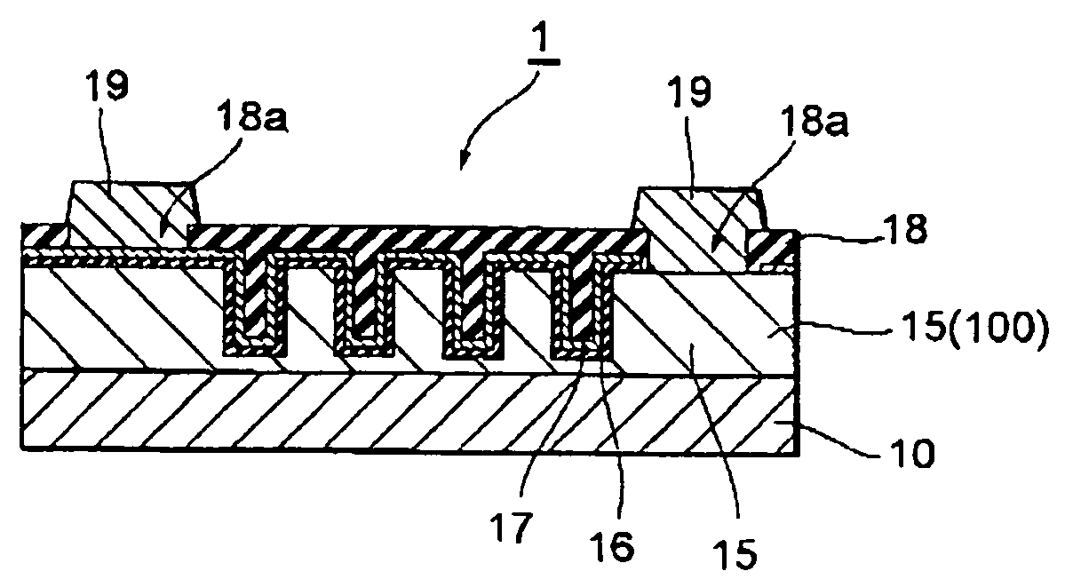
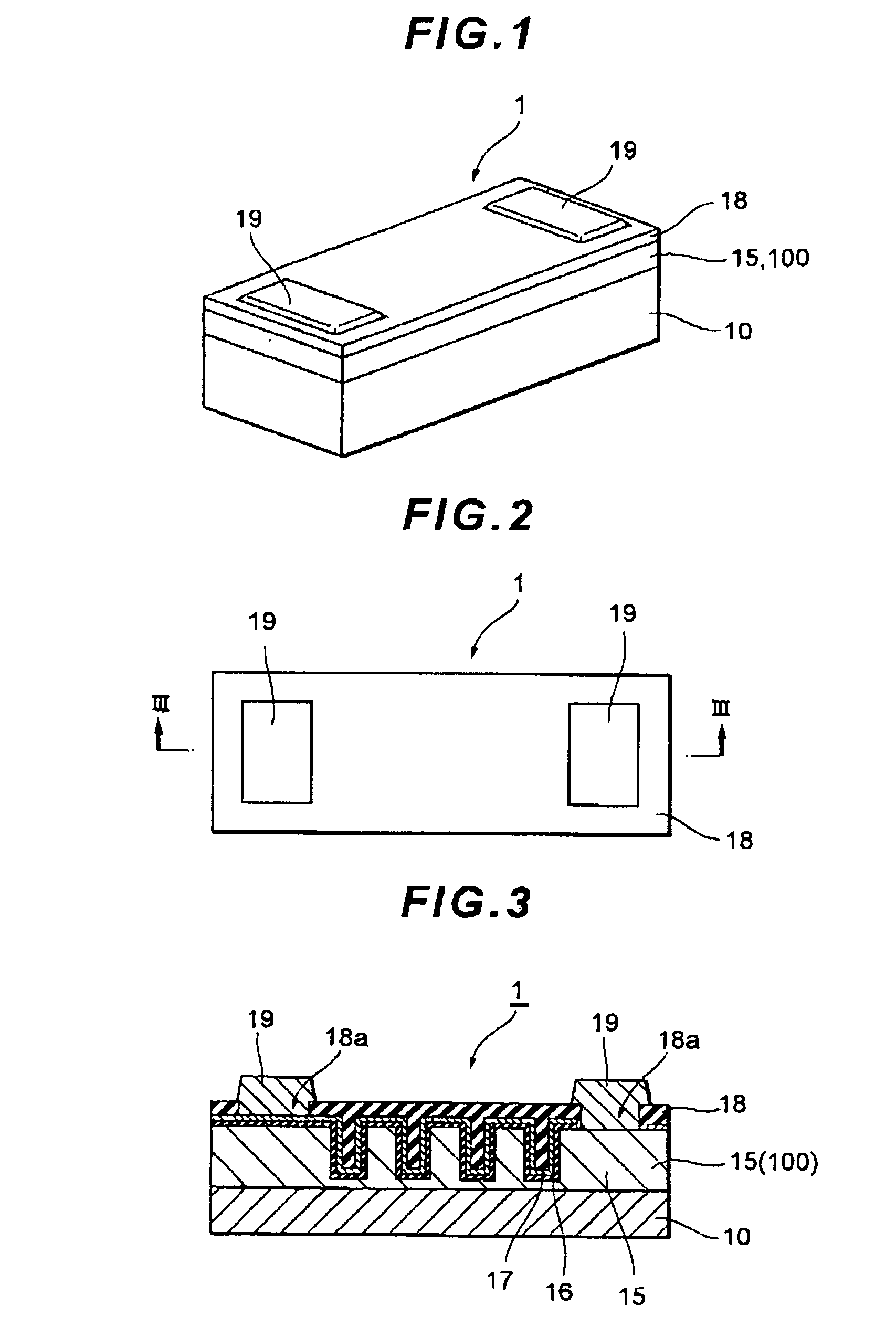
[0067]FIGS. 1 and 2 are a perspective view and a plan view showing the schematic configuration of a preferred embodiment of a thin film capacitor according to the present invention, and FIG. 3 is a cross-sectional view along line III-III in FIG. 2.
[0068]A thin film capacitor 1 in this configurational example has a trench pattern adequately fabricated by the additive method, and has a lower electrode 15 serving as a trench forming layer 100 where a trench pattern is to be formed, a dielectric film 16 so provided as to cover the lower electrode 15, and an upper electrode 17 laminated in order on the entire top surface of a substrate 10 (base substance). As a layer overlying the upper electrode 17, an insulative protection film 18 (passivation film) having two openings 18a is formed therein through which the upper electrode 17 and the lower electrode 15 are respectively exposed. Further, the two openings 18a of the protection film 18 are respectively connected to ...
example 3
CONFIGURATIONAL EXAMPLE 3 OF THIN FILM CAPACITOR
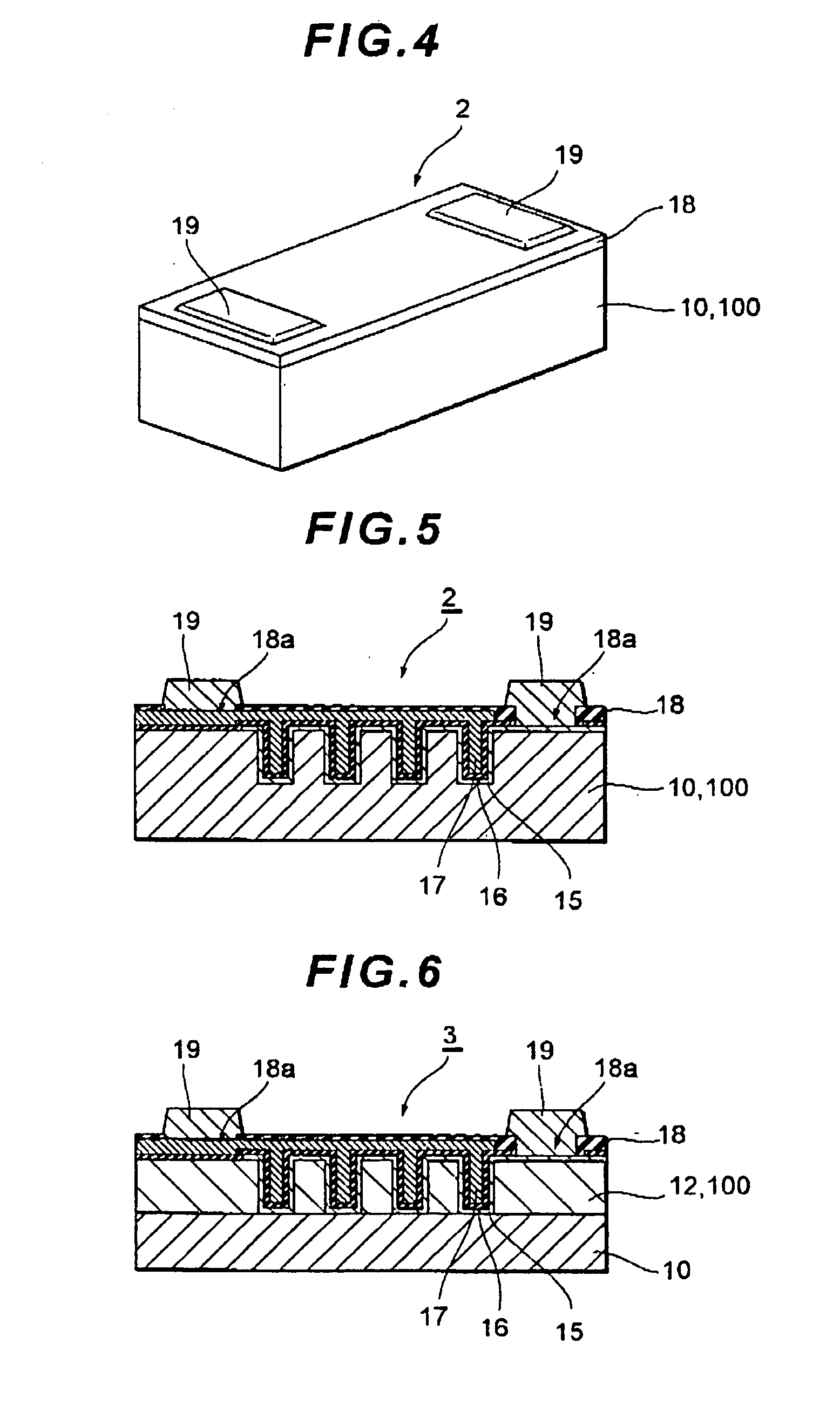
[0072]FIG. 6 is a cross-sectional view showing the schematic configuration of a further preferred embodiment of the thin film capacitor according to the present invention.
[0073]A thin film capacitor 3 in this configurational example has a trench pattern adequately fabricated by the subtractive method, and has an insulating layer 12 serving as a trench forming layer 100 where a trench pattern is to be formed, a lower electrode 15 so provided as to cover the insulating layer 12, a dielectric film 16, and an upper electrode 17 laminated in order on the entire top surface of a substrate 10. As a layer overlying the upper electrode 17, an insulative protection film 18 having two openings 18a is formed therein through which the upper electrode 17 and the lower electrode 15 are respectively exposed. Further, the two openings 18a of the protection film 18 are respectively connected to pad electrodes 19.
[0074]The capacitances of the thin film c...
example 1
FABRICATION EXAMPLE 1 OF THIN FILM CAPACITOR
[0098]One example of the fabrication method for the thus configured thin film capacitor 1 will be described below. FIGS. 17 to 33 are cross-sectional views showing states of fabricating the thin film capacitor 1 (process flow diagrams).
[0099]First, as shown in FIG. 17, the substrate 10 provided with the thin film capacitor 1 is prepared. The substrate 10 is not particularly restrictive, and can be a silicon substrate, a ceramic substrate of alumina or the like, a glass ceramic substrate, a glass substrate, a single crystal substrate of sapphire, MgO, SrTiO3 or the like, or a metal substrate of Fe—Ni alloy or the like, and is preferably a type which chemically and thermally stable, generates less stress and is easy to hold the surface smoothness. When a conductive substrate, such as a metal substrate or silicon substrate, is used as the substrate 10, it is preferable to form an insulating film like an oxide film on the top surface of the su...
PUM
 Abstract
Description
Claims
Application Information
 - Generate Ideas
- Intellectual Property
- Life Sciences
- Materials
- Tech Scout
- Unparalleled Data Quality
- Higher Quality Content
- 60% Fewer Hallucinations
Browse by: Latest US Patents, China's latest patents, Technical Efficacy Thesaurus, Application Domain, Technology Topic, Popular Technical Reports.
© 2025 PatSnap. All rights reserved.Legal|Privacy policy|Modern Slavery Act Transparency Statement|Sitemap|About US| Contact US: help@patsnap.com