
Device and Method for the Demodulation Electromagnetic Wave Fields

a technology of electromagnetic wave field and demodulation device, which is applied in the direction of instruments, television systems, and reradiation, to achieve the effects of less susceptibility, less susceptibility, and improved spatial (lateral) sampling of the scen

Active Publication Date: 2008-10-02
AMS SENSORS SINGAPORE PTE LTD
View PDF1 Cites 39 Cited by
  • Summary
  • Abstract
  • Description
  • Claims
  • Application Information

AI Technical Summary

Benefits of technology

[0014]The pixel device according to the invention is thus capable of demodulating optical waves at very high speed and with high sensitivity at the same time. The transfer of the photo-generated electrons over the potentially large photo-sensitive area of the detection region is mainly accomplished by a lateral, static drift field, which is a constant electric field. That leads to a very fast transportation process in the charge domain and high demodulation frequencies up to the Gigahertz range are reachable without any loss of sensitivity. The in-pixel demodulation process is performed in the almost noise-free charge domain. The requirements to the driving electronics are reduced as well, because any dynamically controlled structure in the pixel have sizes that are as small as possible. The demodulation of the photo-generated charge-flow signal, also called signal of flowing charges or signal of charge flow, is performed by fast activation of conduction channels. These conduction channels have smallest path lengths of charge transport. The fast transportation process and the fast activation of conduction channels, which are transfer means, enable the demodulation of high signal frequencies. Furthermore, the small size of the demodulation area means small parasitic capacitances of the control gates which have to be quickly charged or recharged so that a large number of pixels can be driven with high frequencies at the same time. The overall requirements on the driver electronics are drastically reduced due to the small capacities and hence, the demodulation efficiency is even increased further.
[0019]The pixel device according to the invention is less susceptible against asymmetric demodulation, i.e., an unequal sampling process in the demodulation region. The reason for less susceptibility is that the demodulation process is not influenced anymore by the direction of the light impinging on the pixel. This is even more advantageous if the demodulation region is designed as non-photo-sensitive.
[0020]Another advantage of the demodulation means of the pixel device is the possibility of designing non-stripe-like structures, but square pixel shapes. That leads to a tremendous improvement of spatial (lateral) sampling of the scene and it enables the efficient use of micro-lens arrays. Still another advantage of the pixel device is less distortion of the sampling signal due to delays and attenuations within the demodulation region because the dynamically controlled part of the pixel is kept as small as possible. The large photo-sensitive detection region is controlled statically.
[0021]The pixel device according to the invention is applicable to all kinds of applications where a detection of electromagnetic waves is necessary. Moreover, the pixel device is best-suited for applications where a demodulation of the electromagnetic wave is required, in particular if the wave is an intensity-modulated optical signal. The demodulation capability of the pixel at high frequencies and with high optical sensitivity at the same time makes the pixel extremely suitable for three-dimensional distance measurements with high accuracies. The set-up of complete one- or two-dimensional arrays allows three-dimensional acquisitions in real-time and without any moving parts within the whole system. Any modulation scheme is applicable, i.e., sine-wave modulation, rectangular modulation, coded modulation schemes such as pseudo-noise modulation as well as frequency-modulated signals and chirp signals. However, beside the just mentioned continuous-wave modulation methods, also pulse-modulated schemes are applicable with the pixel device of the present invention.
[0022]The photo-sensitive pixel device according to the present invention enables the sampling of modulated electromagnetic waves, in particular in the optical range, with highest accuracy. It has a compact size and hence, it can be well integrated with additional electronic circuits on one single chip. The special architecture allows for fabricating that pixel in any standard complementary metal oxide semiconductor (CMOS) or charge coupled device (CCD) process with silicon as substrate material, making the fabrication very cost-efficient. Alternative substrate materials, such as silicon germanium and so on, support even higher frequencies.

Problems solved by technology

Furthermore, the small size of the demodulation area means small parasitic capacitances of the control gates which have to be quickly charged or recharged so that a large number of pixels can be driven with high frequencies at the same time.

Method used


Image

  • Device and Method for the Demodulation Electromagnetic Wave Fields
  • Device and Method for the Demodulation Electromagnetic Wave Fields
  • Device and Method for the Demodulation Electromagnetic Wave Fields

Examples


Embodiment Construction

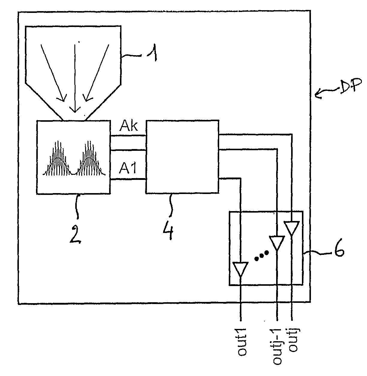
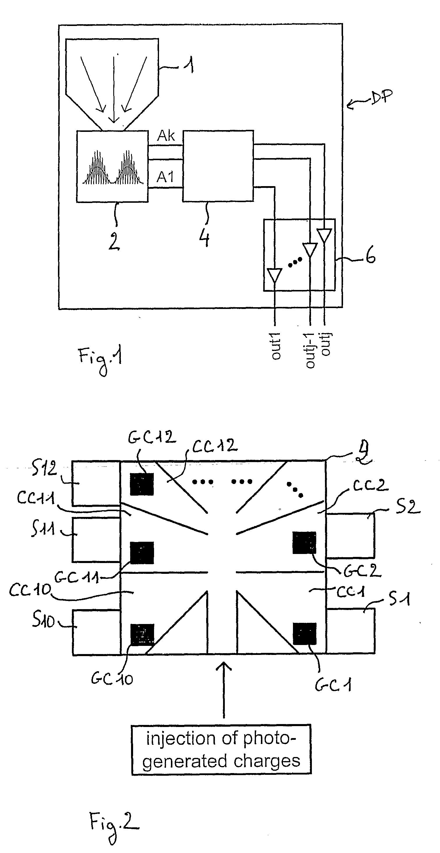
[0038]FIG. 1 shows a photo-sensitive pixel according to the invention. This photo-sensitive pixel DP comprises a photo-sensitive detection region 1, a demodulation region 2, an optional stage 4 for any kind of data processing and optionally amplification circuitry 6. On reception of electromagnetic radiation, e.g. light radiation, on the photo-sensitive area of the detection region 1 and potentially of the demodulation region 2, photo charge carriers are generated.

[0039]The detection region 1, in particular if largely designed, needs to transport the photo-generated charge carriers to the demodulation region 2 as fast as possible in order to minimize any low-pass filtering effects on the opto-electronically converted signal, also called electric signal of flowing charges or photo-current signal. The fast charge-carrier transport to the demodulation region 2 is realized by a lateral drift field into the particular direction. That drift field can be generated by various methods. The f...


PUM

PropertyMeasurementUnit
semiconductoraaaaaaaaaa
electromagnetic wave fieldaaaaaaaaaa
timeaaaaaaaaaa

Abstract

A new pixel in semiconductor technology comprises a photo-sensitive detection region (1) for converting an electromagnetic wave field into an electric signal of flowing charges, a separated demodulation region (2) with at least two output nodes (D10, D20) and means (IG10, DG10, IG20, DG20) for sampling the charge-current signal at at least two different time intervals within a modulation period. A contact node (K2) links the detection region (1) to the demodulation region (2). A drift field accomplishes the transfer of the electric signal of flowing charges from the detection region to the contact node. The electric signal of flowing charges is then transferred from the contact node (K2) during each of the two time intervals to the two output nodes allocated to the respective time interval. The separation of the demodulation and the detection regions provides a pixel capable of demodulating electromagnetic wave field at high speed and with high sensitivity.

Description

FIELD OF THE INVENTION[0001]The present invention relates to a pixel device for the detection and the demodulation of modulated electromagnetic waves, in particular waves of frequencies within the optical frequency spectrum, according to the preambles of the independent claims.[0002]The pixel device can be exploited in all applications demanding high photo-sensitive pixel coupled with fast samplings on-pixel. These pixel characteristics are especially sought for demodulating temporally intensity-modulated electromagnetic light waves. Such pixels are particularly interesting for non-contact distance measuring sensors based on the time-of-flight principle or interferometry but as well as in phase-measuring bio (chemical) applications such as fluorescence applications.BACKGROUND OF THE INVENTION[0003]In the German patent DE4440613C1 (Spirig, “Vorrichtung und Verfahren zur Detektion eines intensitätsmodulierten Strahlungsfeldes”, 1996), a demodulation device is presented which samples t...

Claims


Application Information

Patent Timeline
Patent Type & Authority Applications(United States)
IPC IPC(8): G02F2/00
CPCG01S7/4863H01L31/02005H01L27/14603G01S17/89G01S17/894H04N25/77H04N25/771H04N25/772H04N5/66
Inventor BUETTGEN, BERNHARD
Owner AMS SENSORS SINGAPORE PTE LTD
Learn More