Interposer and method for producing the same and electronic device

a technology of electronic devices and interposers, which is applied in the field of interposers, can solve the problems of high device cost, inconvenient increase of production cost, long process time, etc., and achieve the effects of short and simple production process, improved device reliability, and reduced production cos

Inactive Publication Date: 2008-10-02
SHINKO ELECTRIC IND CO LTD
View PDF2 Cites 57 Cited by
  • Summary
  • Abstract
  • Description
  • Claims
  • Application Information

AI Technical Summary

Benefits of technology

[0006]It is an object of the present invention to solve the above-described problems of the usual interposer made of the silicon substrate and to provide an interposer in which producing processes are short and simple, a production can be carried out without using expensive devices such as a CMP polishing machine, a CVD device, a sputtering device or the like, and a multi-layer structure can be easily realized and a package can be serviceably miniaturized.
[0007]Further, it is another object of the present invention to provide a method in which the above-described interposer can be produced in short and simple processes by using an inexpensive and general-purpose producer in place of an expensive producer.
[0008]Further, it is still another object of the present invention to provide an electronic device provided with the interposer and satisfying requirements such as a compactness, a thin structure, a high performance and a high density mounting.
[0023]As can be understood from a below-described detailed explanation, according to the present invention, since the imprint technique, particularly, the nano imprint technique is introduced differently from the usual method for producing the interposer made of the silicon substrate, the interposer can be produced in short and simple producing processes. Further, in producing the interposer, since expensive devices such as the CMP polishing machine, the CVD device using a vacuum process, the sputtering device or the like do not need to be employed as in a usual case, a production cost can be greatly serviceably reduced. Further, the through wiring can be formed by a fine pattern and a dimensional error can be restricted to an extremely low level, so that a wiring density and the reliability of the device can be improved. Still further, the multi-layer structure of the interposer can be easily realized, which can contribute to the high density mounting and the miniaturization of the package.
[0024]Further, according to the present invention, the electronic device can be provided that satisfies requirements such as a compactness, a thin form, a high performance and a high density mounting or the like.

Problems solved by technology

However, when these systems are carried out, the processes are undesirably long and complicated and a production cost is inconveniently increased.
Further, especially, since a CMP polishing machine, a CVD device and a sputtering device need to be employed, a problem arises that the cost of devices is high.
Further, since the processes are complicated, a problem arises that a package is hardly miniaturized due to a multi-layer structure.

Method used


Image

  • Interposer and method for producing the same and electronic device
  • Interposer and method for producing the same and electronic device
  • Interposer and method for producing the same and electronic device

Examples


example 1

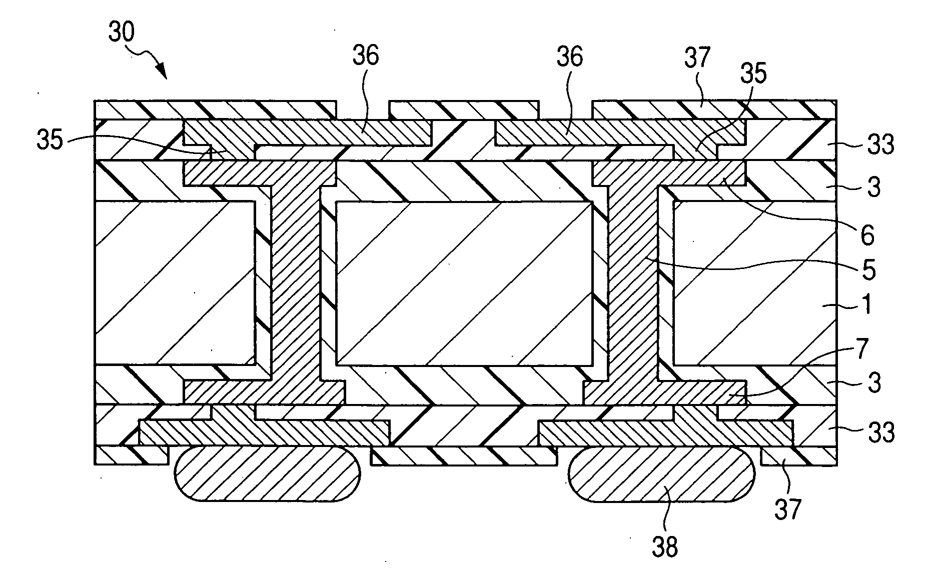
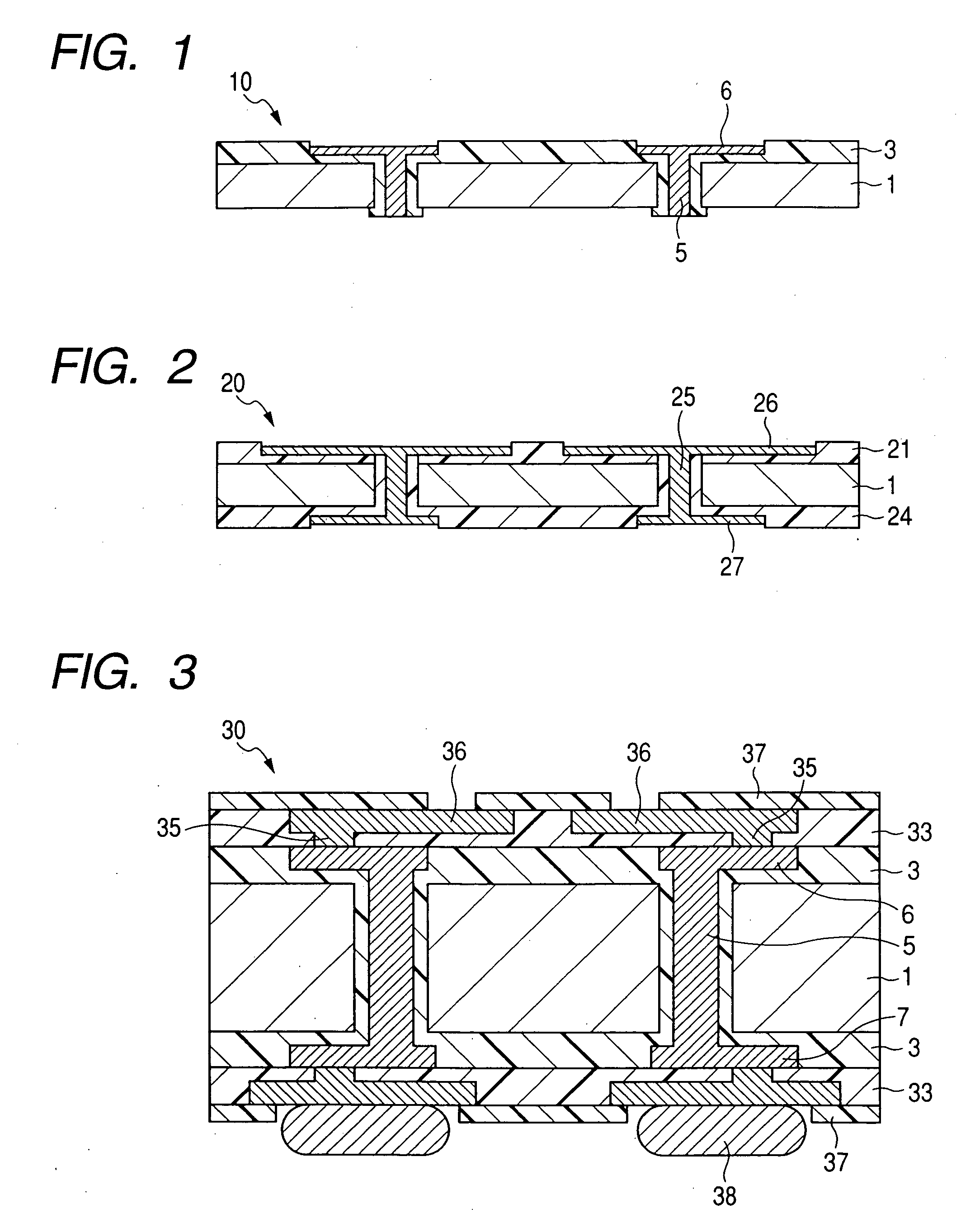
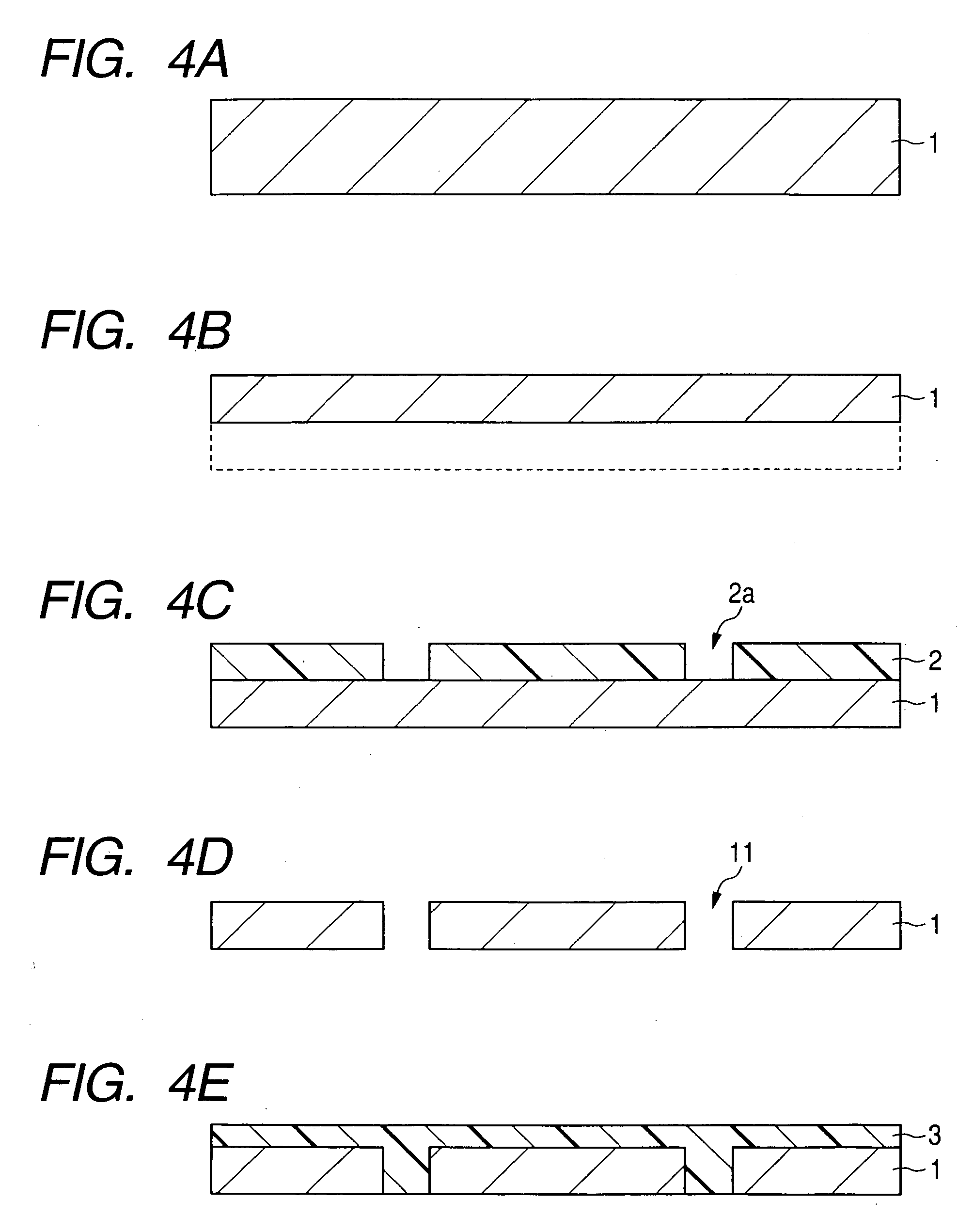
[0049]In this example, the production of the interposer for the semiconductor device shown in FIG. 1 will be described by referring to FIGS. 4A to FIG. 4I.

[0050]Initially, as shown in FIG. 4A, a silicon wafer 1 having a prescribed size (in this example, thickness of 625 μm) is prepared.

[0051]Then, to set the thickness of the silicon wafer 1 to 200 μm, as shown in FIG. 4B, a back surface is polished. A back surface polishing process can be performed by using a back surface polishing machine sold at a market. In the drawing, a part shown by a dotted line is removed.

[0052]After the silicon wafer 1 having the thickness of 200 μm is manufactured, a resist excellent in its etching resistance is applied to the surface of the silicon wafer 1. After the resist is hardened, the resist is patterned. As shown in FIG. 4C, the silicon wafer 1 having a resist pattern 2 is obtained. Here, an opening 2a of the resist pattern 2 is provided to form a through wiring in a process of a post-stage. The di...

example 2

[0058]In this example, the production of the interposer for the semiconductor device shown in FIG. 2 is described with reference to FIGS. 5A to 5K.

[0059]Firstly, as shown in FIG. 5A, a silicon wafer having a prescribed size (in this example, thickness of 50 μm) is prepared.

[0060]Then, to form a first interlayer insulating film having a first preliminary wiring pattern in a process of a post-stage, the process shifts to a first imprint process. Firstly, as shown in FIG. 5B, for instance, a thermoplastic resin or a ultraviolet ray curing resin (in this example, polyimide resin) is applied to the upper surface of the silicon wafer 1 by a screen printing process to forma first insulating resin layer 21 with the thickness of 5 μm.

[0061]After the insulating resin layer 21 is formed as described above, a separately prepared first nano metal mold 41 is pressed to the first insulating resin layer 21. The first nano metal mold 41 is manufactured by finely processing, for instance, nickel, sil...


PUM


Abstract

An interposer includes a substrate made of an inorganic material; a through wiring including conductors embedded in through holes; and an upper wiring and (or) a lower wiring. The through wiring, the upper wiring and the lower wiring are respectively formed on preliminary wiring patterns that are additionally simultaneously or sequentially formed on layers made of an insulating material applied to at least wiring forming parts of the substrate, and are formed with a metal mold itself used for forming the preliminary wiring patterns or layers made of a wiring material applied by a printing operation, a plating operation or a deposition on the preliminary wiring patterns formed on the layers of the insulating material by transferring a fine structure pattern of the metal mold.

Description

BACKGROUND OF THE INVENTION[0001]The present invention relates to an interposer and more particularly to an interposer (it is also referred to as an interposer board) that is interposed between a wiring board and an electronic element (for instance, a semiconductor chip) mounted on the wiring board and used to form a semiconductor device or other electronic devices. The present invention also relates to a method for producing such an interposer and a semiconductor device or other electronic devices in which the interposer is incorporated.[0002]As well known, the semiconductor device is formed by mounting a semiconductor chip such as an IC chip or an LSI chip on a wiring board, for instance, a multi-layer circuit board. Further, to meet the miniaturization of the semiconductor device, the interposer is frequently interposed between the wiring board and the semiconductor chip. For instance, Patent Document 1 discloses a semiconductor device in which a semiconductor chip is faced down ...

Claims


Application Information

Patent Timeline
Patent Type & Authority Applications(United States)
IPC IPC(8): H01L21/00
CPCH01L21/486H01L21/4867H01L23/49827H05K1/0306H05K3/005H05K3/4053H05K3/445H05K2203/0108H01L2924/0002H01L2924/00
Inventor SUNOHARA, MASAHIROTAGUCHI, YUICHI
Owner SHINKO ELECTRIC IND CO LTD
Why Eureka
Try Eureka