Semiconductor device, LED head and image forming apparatus

a technology of led head and semiconductor device, which is applied in the direction of semiconductor device, electrical apparatus, basic electric elements, etc., can solve the problems of reducing the effect of diffuse heat, affecting the characteristic and reliability of semiconductor devices, etc., and achieves efficient diffusion of heat produced, shortening the distance between the active layer, and high heat conductivity. high efficiency

Inactive Publication Date: 2008-10-16
OKI DATA CORP
View PDF15 Cites 26 Cited by
  • Summary
  • Abstract
  • Description
  • Claims
  • Application Information

AI Technical Summary

Benefits of technology

[0013]According to the present invention, because only a thin diamond-like carbon layer is furnished between a substrate and a semiconductor thin film layer so as to shorten a distance between a active layer and the substrate, a heat conduction from the active layer which is a main heat producing region to the substrate whose heat conductivity is high becomes high efficient. Here, because the diamond-like carbon layer is thin, it is impossible that the efficiency of heat conduction in a thickness direction drops. As a result, it is possible to efficiently diffuse the heat produced by the semiconductor element toward the external, and prevent the temperature of the semiconductor device from rising. Therefore, it is possible to improve the operation characteristic of the semiconductor device and to sustain a stable operation.
[0014]The above and other objects and features of the present invention will become apparent from the following detailed description and the appended claims with reference to the accompanying drawings.

Problems solved by technology

Then, a temperature rise of the semiconductor element brings on a bad influence with respect to characteristic and reliability of semiconductor device.
However, in the above-stated technology, a problem exists, that is, because the sapphire substrate intervenes between a light emitting region and the diamond substrate, a distance between a main heat producing region and material with high heat conductivity becomes far, so that an effect to diffuse heat is dropped.

Method used


Image

  • Semiconductor device, LED head and image forming apparatus
  • Semiconductor device, LED head and image forming apparatus
  • Semiconductor device, LED head and image forming apparatus

Examples


embodiment 1

[0089]In the embodiment, a structure is adopted to set a distance between a main heat producing region and a substrate with high heat conductivity as short as possible so as to efficiently conduct heat energy toward external of semiconductor device.

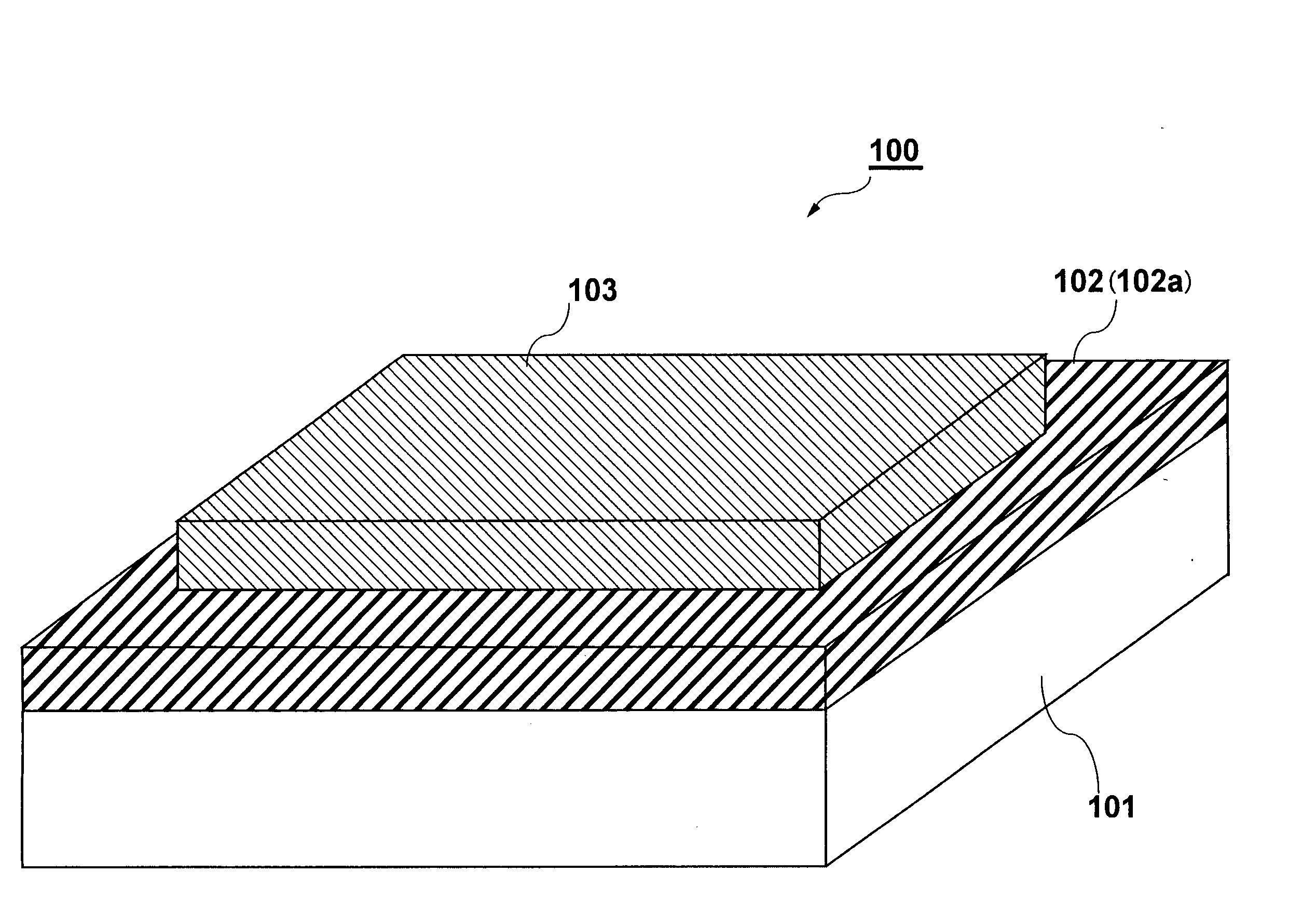
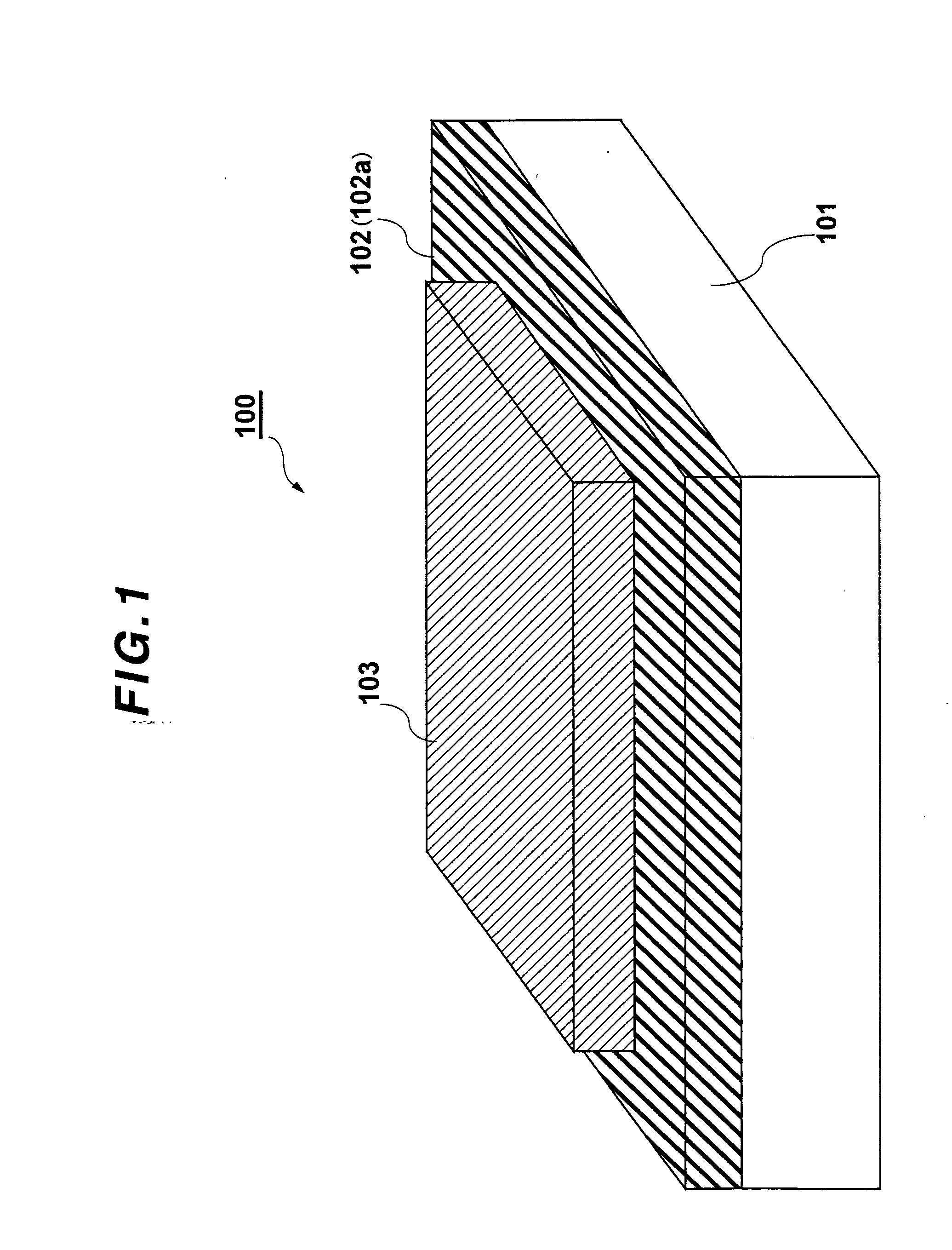
[0090]FIG. 1 is a cubic diagram showing a semiconductor device in embodiment 1 of the present invention; and FIG. 2 is a cross section showing a semiconductor device in embodiment 1 of the present invention.

[0091]As shown by the FIGS. 1 and 2, in a semiconductor device 100 in embodiment 1, a surface coating layer 102 covers a surface of a metallic substrate 101, on the surface coating layer 102, a semiconductor thin film layer 103 is stuck. Though a structure of the semiconductor thin film layer 103 is not shown in the FIG. 2, the semiconductor thin film layer 103 is a semiconductor thin film comprising semiconductor element. The semiconductor element may be, for example, light emitting diode, semiconductor laser, integrated circuit, sens...

embodiment 2

[0168]In the embodiment, as compared with the structure of the embodiment 1, a metal layer with high light reflectance is added to be separately furnished on a metallic substrate, in order to improve light emitting efficiency of light emitting element.

[0169]FIG. 39 is a plane diagram showing a LED device in embodiment 2 of the present invention; and FIG. 40 is a magnification diagram of A-A section in FIG. 39.

[0170]The following is to explain the embodiment 2 by referring to the two drawings.

[0171]As shown by the FIG. 39, a symbol 411 represents a first electroconductive side GaAs layer (contact layer); a symbol 415 represents a second electroconductive side GaAs layer (contact layer); and a symbol 417 represents a second electroconductive side electrode. Further, a symbol 417b represents second electroconductive side wiring; and a symbol 417c represents a second electroconductive side connection pad. Furthermore, a symbol 418b represents first electroconductive side wiring; a symbo...

embodiment 3

[0183]In the embodiment, as compared with the structure of the embodiments 1 and 2, a semiconductor thin film is furnished on a freestanding substrate of diamond-like carbon so as to more improve heat liberating effect.

[0184]FIG. 42 is a cross section showing a semiconductor device in embodiment 3 of the present invention.

[0185]As shown by the FIG. 39, a symbol 501 represents a diamond-like carbon substrate. Regarding a surface flatness of the diamond-like carbon substrate, it is desired such as that in embodiment 1. That is, the average value of surface roughness Ra≦5 nm, the maximum roughness RPV≦10 nm, the maximum undulation Rmax≦ 1 / 1000, best is that the average value of surface roughness Ra≦3 nm, the maximum roughness RPV≦5 nm.

[0186]FIG. 43 is a cross section showing a LED element in embodiment 3 of the present invention.

[0187]The FIG. 43 shows a concrete example of the semiconductor thin film layer 510 of the embodiment 3. As shown by the FIG. 43, a LED element 450 of the embo...


PUM

PropertyMeasurementUnit
wavelength bandaaaaaaaaaa
reflectanceaaaaaaaaaa
roughnessaaaaaaaaaa

Abstract

A semiconductor device is supplied which is able to efficiently liberate heat produced by semiconductor element toward external, prevent temperature rise, improve operation characteristic and maintain stable operation. The semiconductor device comprises a substrate and a semiconductor thin film layer which is accumulated on the substrate and contains semiconductor element, the substrate is a metal substrate, between the metal substrate and the semiconductor thin film layer, a diamond-like carbon layer with high heat conductivity and good insulativity is furnished as a surface coating layer.

Description

BACKGROUND OF THE INVENTION[0001]1. Field of the Invention[0002]The invention relates to a semiconductor device, a LED head and an image forming apparatus; in particular, relates to a semiconductor device, a LED head and an image forming apparatus that can improve characteristic and reliability through effectively diffuse heat caused from semiconductor element.[0003]2. Related Background Art[0004]Semiconductor element produces heat when operating. Further, in the semiconductor element, region which most produces heat is operating region. For example, if the semiconductor element is a light emitting diode, a light emitting region near to PN junction or of an active layer becomes a light emitting center. Then, a temperature rise of the semiconductor element brings on a bad influence with respect to characteristic and reliability of semiconductor device. In order to eliminate the bad influence, it is important to efficiently conduct the heat energy produced by the semiconductor element...

Claims


Application Information

Patent Timeline
Patent Type & Authority Applications(United States)
IPC IPC(8): H01L33/00H01L33/32H01L33/08H01L33/64
CPCH01L33/641H01L33/642H01L2924/0002H01L2924/00
Inventor OGIHARA, MITSUHIKOSAGIMORI, TOMOHIKOSUZUKI, TAKAHITOFUJIWARA, HIROYUKIIGARI, TOMOKISAKUTA, MASAAKI
Owner OKI DATA CORP
Why Eureka
Try Eureka