Semiconductor device

a technology of semiconductor devices and semiconductors, applied in semiconductor devices, semiconductor/solid-state device details, electrical equipment, etc., can solve the problems of reducing the size of the device as a whole, and affecting the operation of the devi

Active Publication Date: 2008-10-23
SEMICON COMPONENTS IND LLC
View PDF61 Cites 13 Cited by
  • Summary
  • Abstract
  • Description
  • Claims
  • Application Information

AI Technical Summary

Problems solved by technology

Therefore, it is difficult to reduce the size of the device as a whole.
Furthermore, since recent semiconductor dies operate fast, high frequency (frequency of several hundreds MHz or more) electromagnetic noise is likely to increase by a high speed switching operation of a transistor to degrade operation characteristics.
However, the wiring may be extended long for a layout design in some cases, and when the semiconductor die and the capacitor element are individual components there is a limitation on the adjacent formation of these.
As described above, the structure having the external capacitor element has a problem of difficulty in realizing both the size reduction of the semiconductor device and the reduction of an influence of electromagn

Method used


Image

  • Semiconductor device
  • Semiconductor device
  • Semiconductor device

Examples


first embodiment

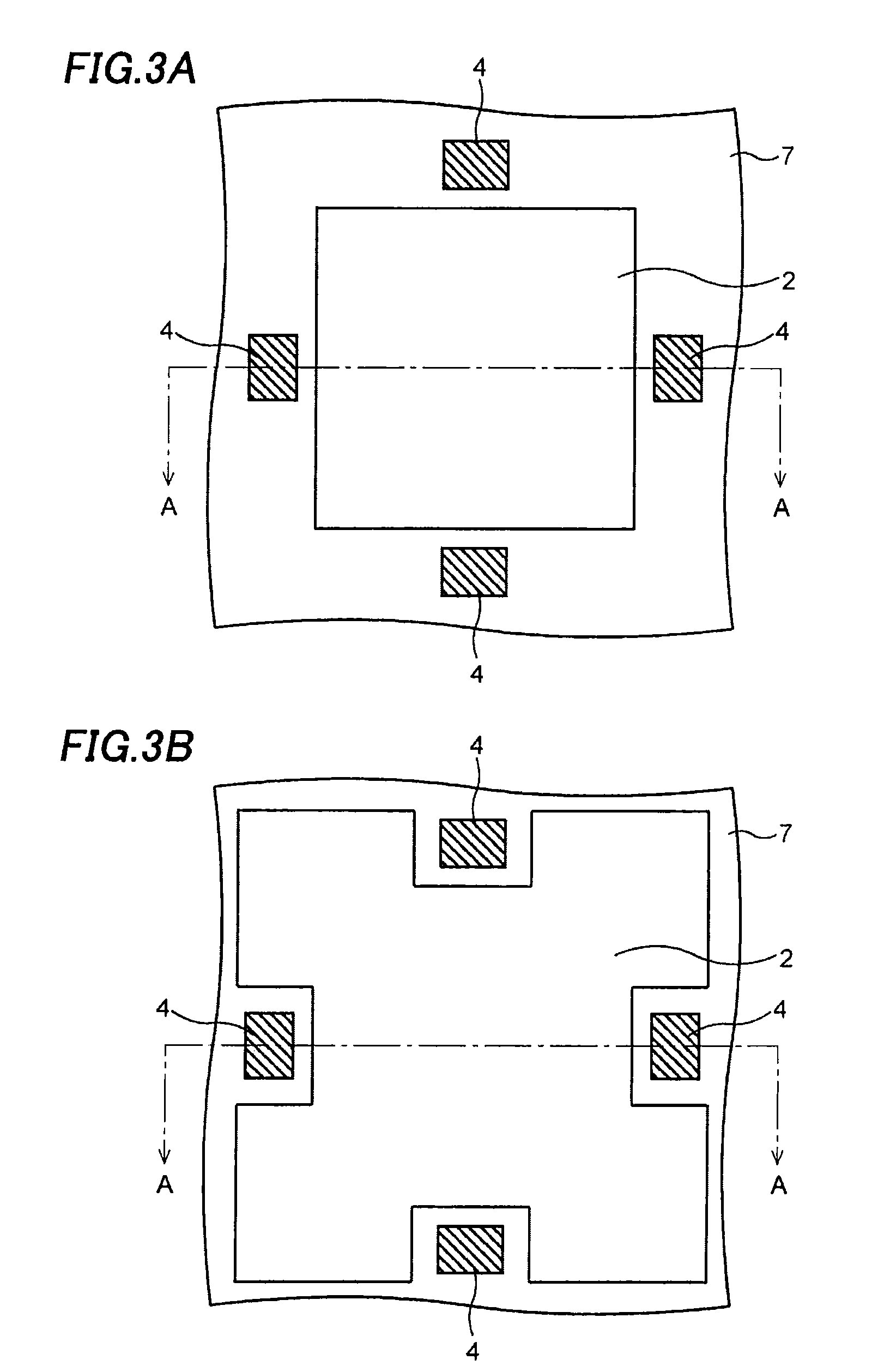
[0030]the invention will be described referring to figures. FIGS. 1 to 9 are cross-sectional views and plan views showing a process of manufacturing a semiconductor device in order. The manufacturing process described below is performed using a wafer form semiconductor substrate and a number of semiconductor devices are formed in a matrix configuration along predetermined dicing lines as borders, although the description is given about a process of forming one of these semiconductor devices for convenience.

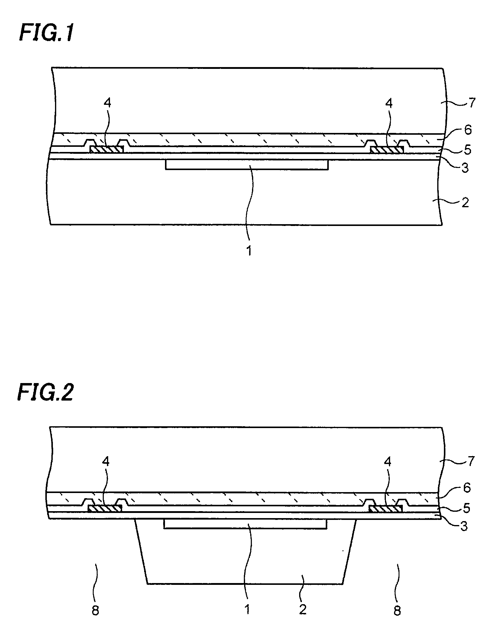
[0031]First, as shown in FIG. 1, a semiconductor substrate 2 made of silicon (Si) or the like is prepared, of which the front surface is formed with a semiconductor integrated circuit 1 (e.g. a driver circuit or a logic circuit formed by integrating semiconductor elements such as a light receiving element such as a CCD sensor, a CMOS sensor or an illumination sensor, a light emissive element or a transistor, wirings connected to these, or the like). The semiconductor substrate 2 i...

third embodiment

[0057]Next, the invention will be described referring to figures. The same numerals are given to the same components as those of the above described embodiments and a description thereof is omitted.

[0058]In a semiconductor device of the third embodiment, as shown in FIG. 12, via holes 30 are formed from the back surface of the semiconductor substrate 2 to the pad electrodes 4, barrier metal layers 31 are formed in the via holes 30 and on the back surface of the semiconductor substrate 2, and the wiring layers 11 made of metal such as aluminum, copper or the like are formed on the barrier metal layers 31. The barrier metal layers 31 are made of a metal material such as, for example, a titanium (Ti) layer, a titanium nitride (TiN) layer, a tantalum (Ta) layer, a tantalum nitride (TaN), a titanium tungsten (TiW) layer or the like, and connected to the pad electrodes 4 on the bottoms of the via holes 30 (near the front surface of the semiconductor substrate 2).

[0059]The capacitor electr...

fourth embodiment

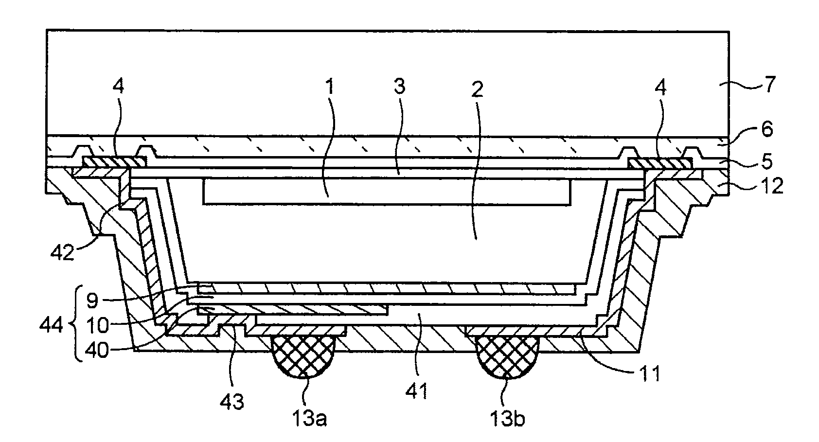
[0062]In the semiconductor device of the fourth embodiment, a wiring layer 40 is formed on the second insulation film 10 on the back surface of the semiconductor substrate 2 so as to overlap the capacitor electrode 9. A third insulation film 41 made of a silicon oxide film, a silicon nitride film or the like is formed so as to cover the wiring layer 40 and the second insulation film 10, and the wiring layers 42, 11 connected to the pad electrodes 4 are formed on the third insulation film 41 along the side and back surfaces of the semiconductor substrate 2. An opening 43 is formed in a portion of the third insulation film 41, reaching the wiring layer 40, and the wiring layer 40 and the wiring layer 42 are connected through this opening 43.

[0063]In the semiconductor device of the fourth embodiment, the capacitor electrode 9, the second insulation film 10 and the wiring layer 40 are layered on the back surface of the semiconductor substrate 2 in this order, and thus these form a capac...


PUM


Abstract

The invention provides a semiconductor device which has a capacitor element therein to achieve size reduction of the device, the capacitor element having larger capacitance than conventional. A semiconductor integrated circuit and pad electrodes are formed on the front surface of a semiconductor substrate. A second insulation film is formed on the side and back surfaces of the semiconductor substrate, and a capacitor electrode is formed between the back surface of the semiconductor substrate and the second insulation film, contacting the back surface of the semiconductor substrate. The second insulation film is covered by wiring layers electrically connected to the pad electrodes, and the wiring layers and the capacitor electrode overlap with the second insulation film being interposed therebetween. Thus, the capacitor electrode, the second insulation film and the wiring layers form capacitors.

Description

CROSS-REFERENCE OF THE INVENTION[0001]This application claims priority from Japanese Patent Application No. 2007-112336, the content of which is incorporated herein by reference in its entirety.BACKGROUND OF THE INVENTION[0002]1. Field of the Invention[0003]The invention relates to a semiconductor device having a capacitor element.[0004]2. Description of the Related Art[0005]In order to reduce variation of a voltage level by influence of electromagnetic noise to prevent malfunction of a semiconductor die, a capacitor element called a bypass capacitor has been mounted on a terminal (a source terminal or a ground terminal) of a semiconductor die conventionally.[0006]For example, Japanese Patent Application Publication No. Hei 05-021698 discloses a semiconductor device in which a semiconductor die and an external capacitor element called a die capacitor are mounted on the same substrate and packaged in a die form as a whole.[0007]Japanese Patent Application Publication No. 2000-349238 ...

Claims


Application Information

Patent Timeline
IPC IPC(8): H01L29/92
CPCH01L23/3114H01L2224/0401H01L23/5223H01L23/642H01L24/11H01L24/12H01L24/25H01L24/29H01L24/32H01L2224/02313H01L2224/1132H01L2224/131H01L2224/18H01L2924/01013H01L2924/01022H01L2924/01029H01L2924/01033H01L2924/01047H01L2924/01073H01L2924/01074H01L2924/01078H01L2924/01079H01L2924/04941H01L2924/04953H01L2924/09701H01L2924/14H01L2924/19041H01L2924/19043H01L2924/30105H01L2924/30107H01L2924/3011H01L23/481H01L27/14683H01L27/14618H01L2924/014H01L2924/01006H01L2924/01005H01L2924/00013H01L2224/05644H01L2224/0558H01L2224/13099H01L2924/3512H01L2924/00H01L2924/3511
Inventor HORIKOSHI, KATSUUCHIYAMA, HISAYOSHINOMA, TAKASHISEKI, YOSHINORIYAMADA, HIROSHIISHIBE, SHINZOSHINOGI, HIROYUKI
Owner SEMICON COMPONENTS IND LLC
Why Eureka
Try Eureka