Large-Size Glass Substrate For Photomask and Making Method, Computer-Readable Recording Medium, and Mother Glass Exposure Method
a technology of glass substrate and photomask, which is applied in the field of large-scale glass substrate, can solve the problems of reducing the ability to remove moderate irregularities on the substrate surface, reducing the ability of prior art polishing methods to finish to the desired flatness, and reducing the burden of exposure correction. , to achieve the effect of improving the production yield of panels, reducing the burden of exposure correction, and improving the accuracy of exposure correction
- Summary
- Abstract
- Description
- Claims
- Application Information
AI Technical Summary
Benefits of technology
Problems solved by technology
Method used
Image
Examples
example 1
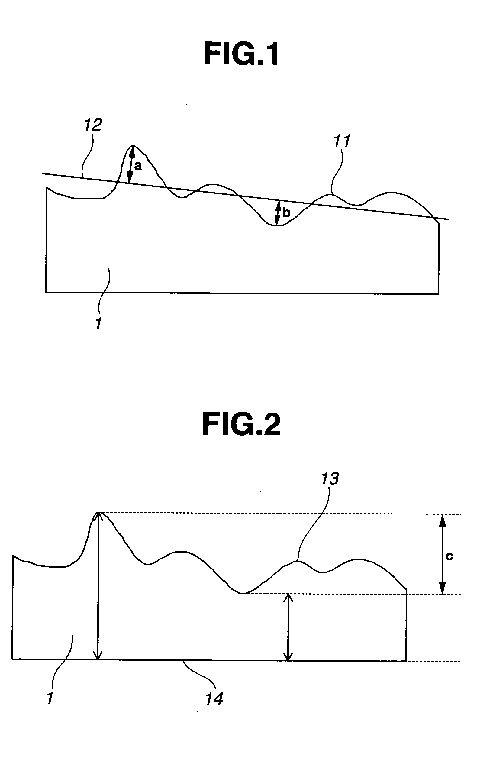
[0096]A starting substrate or substrate stock was furnished by lapping a synthetic quartz glass substrate stock having a size of 330 mm×450 mm (diagonal length ca. 558 mm) and a thickness of 5.3 mm by means of a planetary motion double-side lapping machine using abrasives GC#600 (Fujimi Abrasive Co., Ltd.). The substrate stock had an accuracy as demonstrated by a front surface flatness of 22 μm (surface flatness / diagonal length=39×10−6), a back surface flatness of 25 μm, and a parallelism of 3 μm as measured in the vertical attitude and was of a shape having a higher center portion than the least square plane.
[0097]Then, a deflection of the substrate stock as lapped having a thickness of 5 mm by its own weight when held horizontally was calculated using material strength and the support position of a substrate when held horizontally. A substrate deformation and platen accuracy distortion were previously inspected from a quantity of deformation of a dummy glass substrate stock which ...
example 2
[0106]The procedure of Example 1 was repeated except that a substrate stock having a size of 520 mm×800 mm (diagonal length ca. 954 mm) and a thickness of 10.4 mm was used.
[0107]The proximity gap was measured over substantially the entire region using a laser displacement meter. The measurements of proximity gap included a maximum value of 58 μm and a minimum value of 47 μm, over the entire region excluding the peripheral regions extending 4 cm from the sides, with a gap error of 11 μm.
example 3
[0108]The procedure of Example 1 was repeated except that a substrate stock having a size of 850 mm×1,200 mm (diagonal length ca. 1,471 mm) and a thickness of 10.4 mm was used.
[0109]The proximity gap was measured over substantially the entire region using a laser displacement meter. The measurements of proximity gap included a maximum value of 59 μm and a minimum value of 47 μm, over the entire region excluding the peripheral regions extending 4 cm from the sides, with a gap error of 12 μm.
PUM
| Property | Measurement | Unit |
|---|---|---|
| thickness | aaaaa | aaaaa |
| thickness | aaaaa | aaaaa |
| thickness | aaaaa | aaaaa |
Abstract
Description
Claims
Application Information


