Method of manufacturing SOI substrate

Inactive Publication Date: 2008-10-23
SEMICON ENERGY LAB CO LTD
View PDF35 Cites 42 Cited by
  • Summary
  • Abstract
  • Description
  • Claims
  • Application Information

AI Technical Summary

Benefits of technology

[0011]The top surface of a semiconductor layer of an SOI substrate has irregularities generated by separation from the semiconductor substrate, and thus has low planarity. Therefore, the top surface is irradiated with a laser beam in order to have improve

Problems solved by technology

However, a damage layer produced due to the hydrogen ion implantat

Method used


Image

  • Method of manufacturing SOI substrate
  • Method of manufacturing SOI substrate
  • Method of manufacturing SOI substrate

Examples


example 1

[0118]The present inventors have confirmed that applying laser irradiation can recover the crystallinity of a single-crystalline semiconductor layer to the same level as that of a semiconductor substrate before processed. Further, they have confirmed that the laser irradiation can planarize the surface of the single-crystalline semiconductor layer.

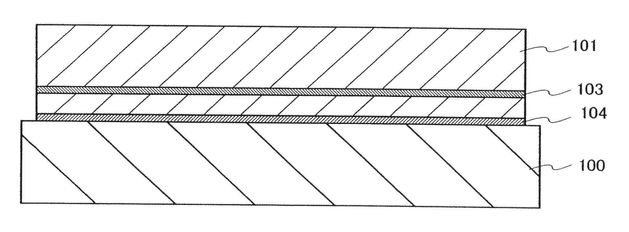
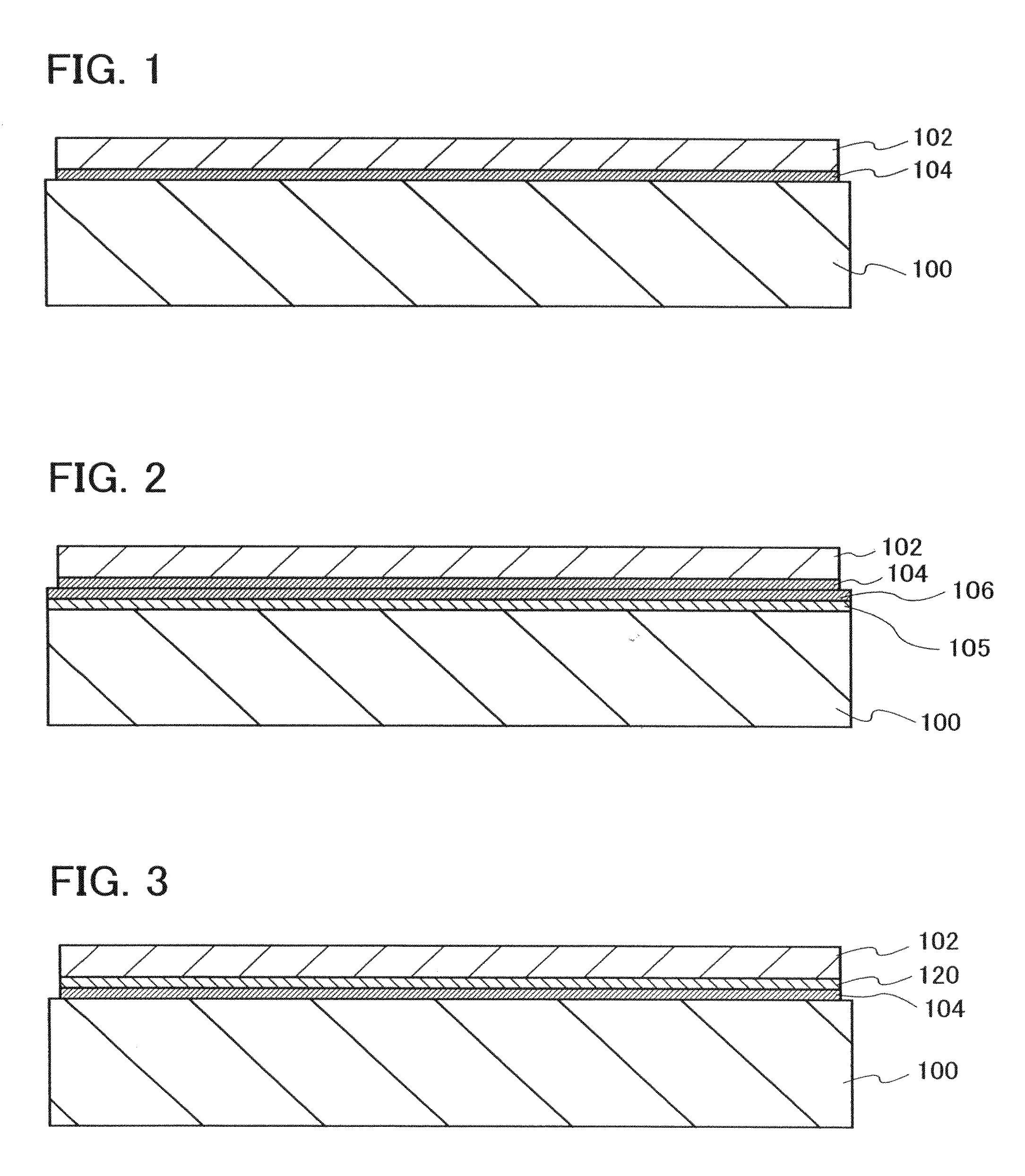
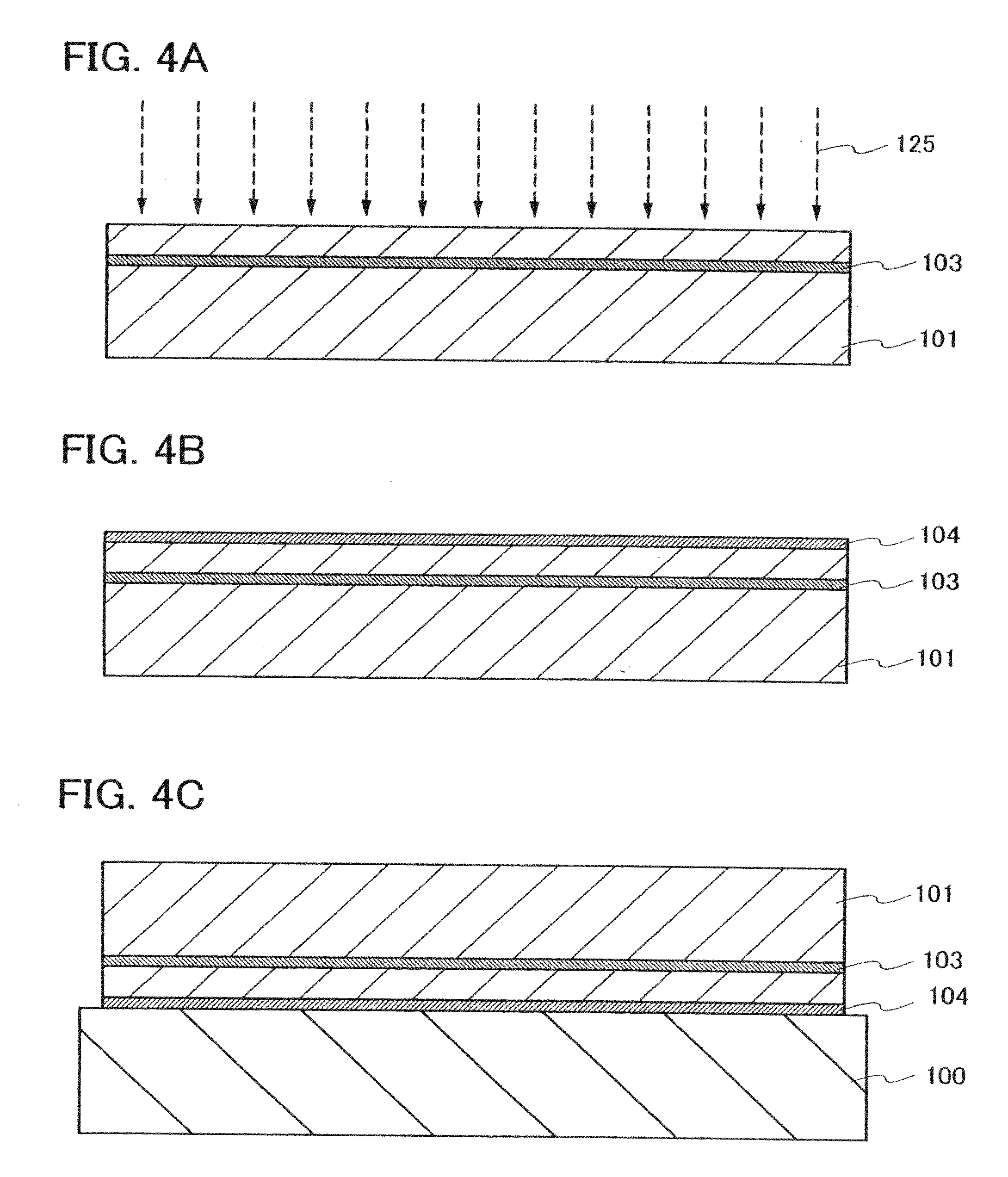
[0119]First, a method of manufacturing an SOI substrate in this example will be described with reference to FIGS. 12A to 12H. FIGS. 12A to 12H are cross-sectional views illustrating a method of manufacturing the SOI substrate. The SOI substrate in this example is a substrate obtained by fixing a single-crystalline layer on a glass substrate.

[0120]A single-crystalline silicon wafer 501 is prepared as a semiconductor substrate (see FIG. 12A). The conductivity type of the wafer is a p type, and the resistivity thereof is about 10 Ω·cm. In addition, the crystal orientation of the main surface is (100).

[0121]First, a silicon oxynitride film 502...

example 2

[0163]A method of forming an ion-implanted layer is described below in Example 2.

[0164]The formation of the ion-implanted layer is conducted by irradiation of a semiconductor substrate with accelerated ions, and the ions are derived from hydrogen (H) (hereafter referred to as “hydrogen ion species”). More specifically, a hydrogen gas or a gas which contains hydrogen in its composition is used as a source gas (a source material); a hydrogen plasma is generated by exciting the source gas; and a semiconductor substrate is irradiated with the hydrogen ion species in the hydrogen plasma. In this manner, the ion-implanted layer is formed in the semiconductor substrate.

(Ions in Hydrogen Plasma)

[0165]In such a hydrogen plasma as described above, hydrogen ion species such as H+, H2+, and H3+ are present. Here are listed reaction equations for reaction processes (formation processes, destruction processes) of the hydrogen ion species.

e+H→e+H++e   (1)

e+H2→e+H2++e   (2)

e+H2→e+(H2)*→e+H+H   (3)

e...


PUM


Abstract

To provide an SOI substrate with an SOI layer that can be put into practical use, even when a substrate with a low allowable temperature limit such as a glass substrate is used, and to provide a semiconductor substrate formed using such an SOI substrate. In order to bond a single-crystalline semiconductor substrate to a base substrate such as a glass substrate, a silicon oxide film formed by CVD with organic silane as a source material is used as a bonding layer, for example. Accordingly, an SOI substrate with a strong bond portion can be formed even when a substrate with an allowable temperature limit of less than or equal to 700° C. such as a glass substrate is used. A semiconductor layer separated from the single-crystalline semiconductor substrate is irradiated with a laser beam so that the surface of the semiconductor layer is planarized and the crystallinity thereof is recovered.

Description

BACKGROUND OF THE INVENTION[0001]1. Field of the Invention[0002]The present invention relates to an SOI (silicon on insulator) substrate. In addition, the present invention relates to a semiconductor device manufactured using the SOI substrate.[0003]Note that a semiconductor device in this specification refers to all devices that can function by utilizing semiconductor characteristics. For example, electro-optic devices, semiconductor circuits, and electronic devices all fall into the category of a semiconductor device.[0004]2. Description of the Related Art[0005]An integrated circuit that uses a semiconductor substrate called an SOI substrate, which is provided with a thin single-crystalline semiconductor layer on an insulating surface, has been developed, replacing a silicon wafer formed by cutting an ingot of a single-crystalline semiconductor into thin slices. Using an SOI substrate can reduce parasitic capacitance between a drain of a transistor and a substrate. Therefore, the ...

Claims


Application Information

Patent Timeline
IPC IPC(8): H01L21/762
CPCH01L21/2007H01L21/76254H01L21/302H01L21/268H01L21/84H01L21/20
Inventor YAMAZAKI, SHUNPEIHIGA, EIJINAGANO, YOJIMIZOI, TATSUYASHIMOMURA, AKIHISA
Owner SEMICON ENERGY LAB CO LTD
Why Eureka
Try Eureka