Chemical-Mechanical Polishing of Sic Surfaces Using Hydrogen Peroxide or Ozonated Water Solutions in Combination with Colloidal Abrasive

a technology of hydrogen peroxide or ozonated water solution and colloidal abrasive, which is applied in the direction of polishing compositions with abrasives, grinding machines, manufacturing tools, etc., can solve the problems of affecting the activation of dopants, affecting the subsequent device production steps, and damaged surface materials, etc., to achieve the effect of increasing the process

Inactive Publication Date: 2008-10-23
II VI
View PDF8 Cites 19 Cited by
  • Summary
  • Abstract
  • Description
  • Claims
  • Application Information

AI Technical Summary

Benefits of technology

[0013]In a further embodiment of the process, improvements can be gained by increasing the process temperature. Raising the temperature can be achieved in two ways. The polishing slurries, wafer carrier, wafers and the polishing plate can be heated directly to a higher temperature or the temperature can be raised using a chemical reaction. In the latter case an acidic or basic solution such as sulfuric acid (H2SO4) or potassium hydroxide (KOH) or ammonium hydroxide (NH4OH) may be added to the process in order to stimulate an exothermic reaction, which ultimately raises the temperature at the wafer surface. It is envisioned that this increase in temperature will aid the removal of SiC into solution.

Problems solved by technology

As is well known in the semiconductor art, the abrasive lapping and polishing processes used to produce planar wafers may leave residual surface damage and defects which adversely affect subsequent device production steps.
Epitaxial films formed on such surfaces may develop localized defective regions, and device fabrication may exhibit excessively low yields.
In addition, damaged surface material will affect the activation of dopants intentionally introduced into the surface during any ion implantation step used during device manufacture.
The sub-surface damage is difficult to see optically and is normally revealed by etching, e.g., in the specific case of SiC, by molten KOH etching.
This method is destructive since it renders the surface rough and enhances defects that are present from the SiC growth process.
However, the significantly greater hardness and relative chemical inertness of SiC, particularly the oxidation of carbon, has made the development of an analogous chemical-mechanical polishing process difficult.
Current SiC chemical-mechanical processes are irreproducible or at best slow and expensive.
As a result, the full value of SiC's unique semiconductor properties may not be realized in practice.

Method used


Image

  • Chemical-Mechanical Polishing of Sic Surfaces Using Hydrogen Peroxide or Ozonated Water Solutions in Combination with Colloidal Abrasive
  • Chemical-Mechanical Polishing of Sic Surfaces Using Hydrogen Peroxide or Ozonated Water Solutions in Combination with Colloidal Abrasive

Examples


Embodiment Construction

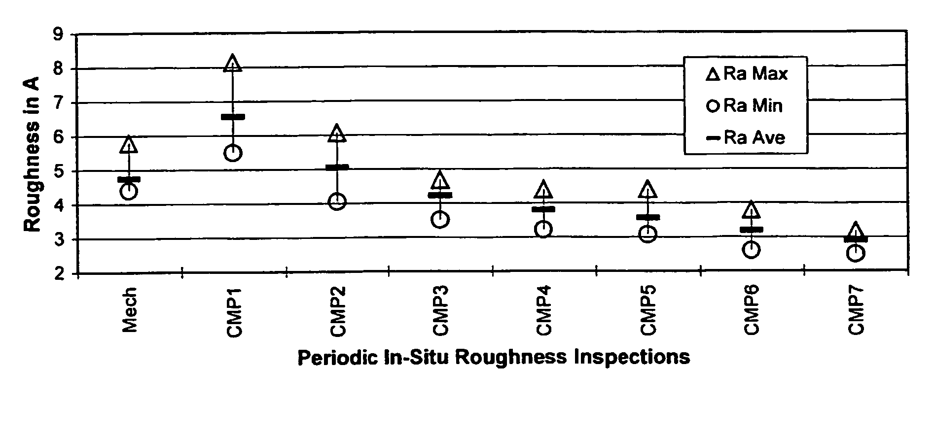
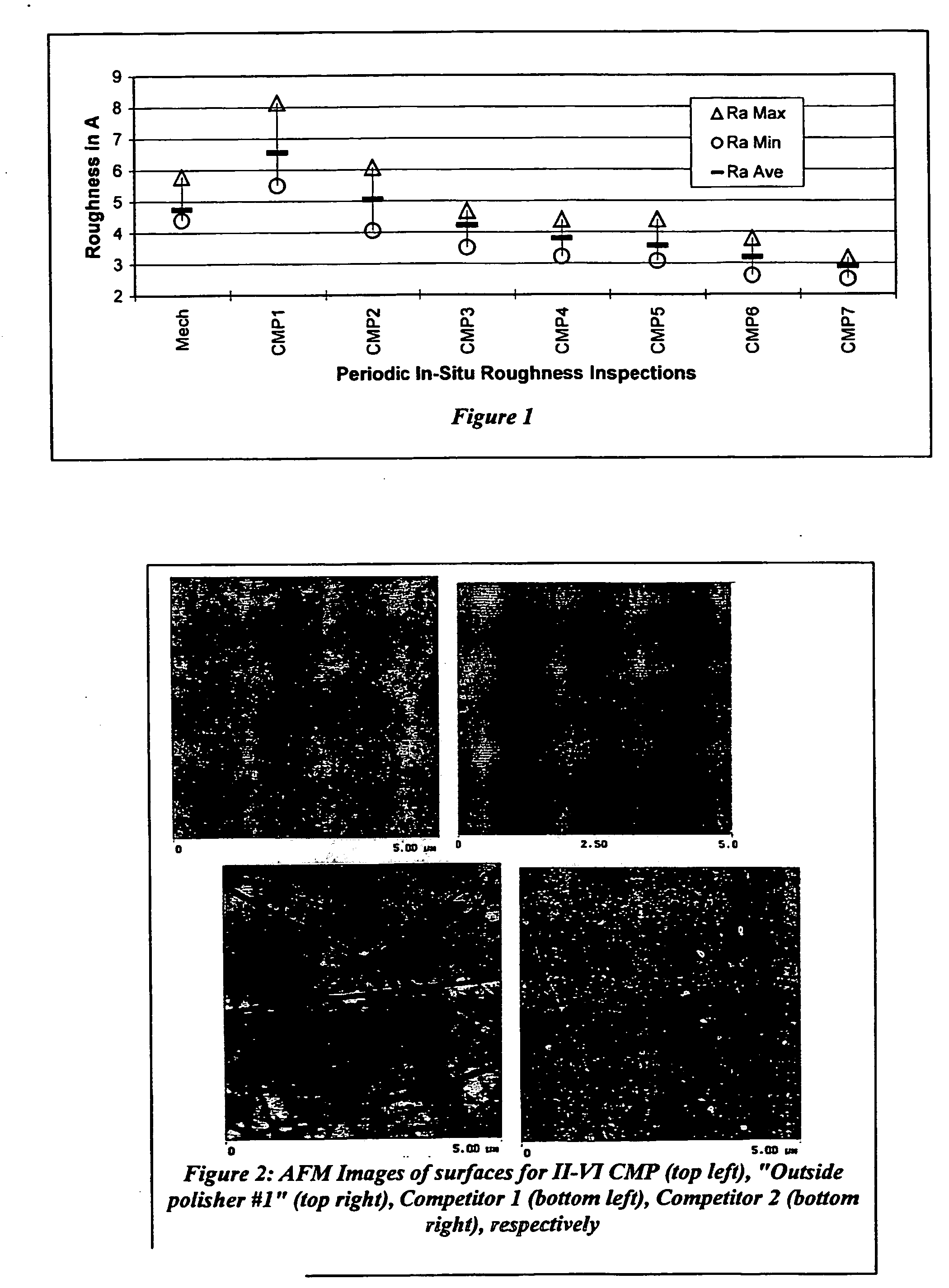
[0017]An important feature of the process taught here lies in the method of oxidation of the surface of a SiC wafer by hydrogen peroxide and / or ozonated water, either separately or in combination. The removal of the oxide is accomplished by the abrasive friction of colloidal silica or alumina or by purely chemical reduction of the oxides in agents, such as HF, without damaging the SiC surface. When used separately or in combination these agents lead to a very planar, extremely low roughness surface (for example, <<3 Angstrom units measured by a Zygo white light interferometry, over a 350 um×250 um field of view, or <0.5 Angstrom units measured by atomic force microscopy (AFM) in a 5×5 um field of view). The resulting surface is also sub-surface damage free.

[0018]The state of the art of SiC polishing elsewhere produces a wafer surface which has a much higher level of surface roughness (3-15 Angstroms) and has evidence of some degree of sub-surface damage. State-of-the-art removal rat...


PUM

PropertyMeasurementUnit
sizeaaaaaaaaaa
temperaturesaaaaaaaaaa

Abstract

A process is taught for producing a smooth, damage-free surface on a SiC wafer, suitable for subsequent epitaxial film growth or ion implantation and semiconductor device fabrication. The process uses certain oxygenated solutions in combination with a colloidal abrasive in order to remove material from the wafer surface in a controlled manner. Hydrogen peroxide with or without ozonated water, in combination with colloidal silica or alumina (or alternatively, in combination with HF to affect the oxide removal) is the preferred embodiment of the invention. The invention also provides a means to monitor the sub-surface damage depth and extent since it initially reveals this damage though the higher oxidation rate and the associated higher removal rate.

Description

BACKGROUND OF THE INVENTION[0001]1. Field of the Invention[0002]The present invention relates to the creation, by chemical-mechanical polishing, of damage-free SiC semiconductor wafer surfaces which are suitable for further epitaxial film growth, ion implantation, and / or subsequent device processing.[0003]2. Description of Related Art[0004]SiC is a semiconductor material with a unique combination of electrical and thermo-physical properties that make it extremely attractive and useful for electronic devices. These properties which include, for example, high breakdown field strength, high practical operating temperature, good electronic mobility and high thermal conductivity, make possible device operation at significantly higher power, higher temperature and with more radiation resistance than comparable devices made from the more conventional semiconductors, silicon and GaAs. It is estimated that transistors fabricated from high resistivity “semi-insulating” SiC will produce over f...

Claims


Application Information

Patent Timeline
Patent Type & Authority Applications(United States)
IPC IPC(8): H01L21/461B24B1/00B24B29/00C09G1/02H01L21/04H01L21/306
CPCC09G1/02H01L21/02024H01L29/66068
Inventor KERR, THOMAS M.MARTIN, CHRISTOPHER T.STEPKO, WALTER R.ANDERSON, THOMAS E.
Owner II VI
Why Eureka
Try Eureka